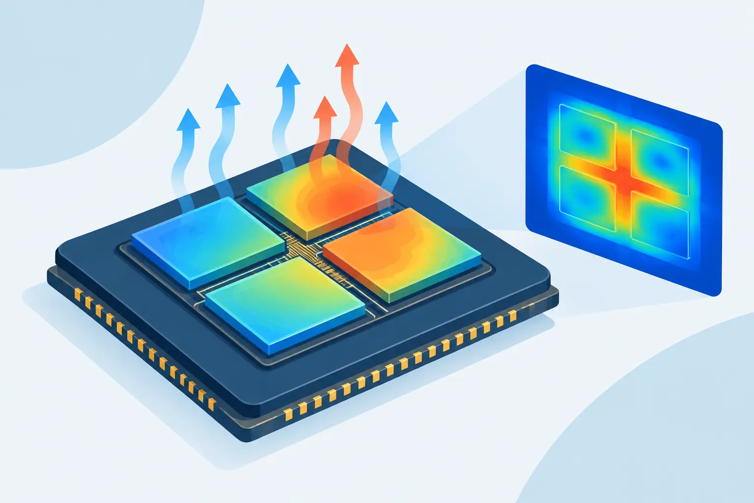
A chiplet assembly can meet its electrical targets and still fail its operating envelope because its thermal path was treated as a package afterthought. In chiplet thermal design, heat is generated in spatially separate dies, crosses several thin and dissimilar interfaces, and is removed through a package whose geometry is rarely uniform. The relevant question is not simply whether total package power is acceptable. It is whether each chiplet, interface, and local interconnect region remains within temperature limits under the workload that produces the highest local dissipation.
Why chiplet assemblies change the thermal problem
A monolithic die has a continuous silicon heat-spreading layer, even if its power density is highly nonuniform. A chiplet-based system divides that layer into separate thermal sources. Compute chiplets, I/O dies, high-bandwidth memory stacks, analog functions, and cache dies may have different thicknesses, footprints, activity factors, and allowable junction temperatures. Their placement establishes thermal coupling before any cooling hardware is selected.
The package adds further complexity. In a 2.5D configuration, heat may spread through microbumps, underfill, an interposer, substrate layers, a lid, thermal interface material, and a heat sink. In a 3D stack, vertical proximity can place a warm logic die beneath a memory die with a lower temperature limit. The effective thermal resistance of the assembly is therefore not a single material property or a single junction-to-ambient value. It is a three-dimensional conduction problem shaped by geometry, material interfaces, and boundary conditions.
Chiplet partitioning also separates electrical and thermal decisions that were formerly made together. Moving an I/O function off a compute die may reduce compute-die power density but can add power sources at the package periphery. Enlarging a chiplet can improve lateral spreading within that die while changing placement options and bump-field density. A thermal model must be available early enough to assess these trade-offs, not only after floorplanning and package selection are fixed.
Chiplet thermal design begins with the correct physical model
The appropriate model depends on the decision being made. Early architecture work may begin with compact representations of each die, assigned power maps, and approximate package layers. That level can expose obvious placement problems, such as placing two peak-power chiplets beneath the same region of the lid. It cannot reliably resolve microbump crowding, narrow bridge structures, or localized hot spots near interfaces.
Detailed analysis requires a three-dimensional representation of the heat path. At minimum, it should include the individual chiplet geometries, active and passive silicon regions where relevant, bump and underfill layers, interposer or bridge structures, package substrate, lid, thermal interface material, and the cooling boundary. Omission is reasonable only when the omitted region has a demonstrably small effect on the result being used for design.
Material properties require the same discipline. Thermal conductivity is often temperature-dependent, and effective conductivity in composite layers is not necessarily the bulk value of any constituent. Underfill and dielectric layers can dominate local vertical resistance despite their small thickness. An interposer may spread heat effectively in one direction while its surrounding dielectric structure limits another path. Treating all layers as isotropic slabs can be useful for a first estimate, but it should not be mistaken for a resolved package model.
Power maps are model inputs, not fixed labels
A chiplet power number is insufficient for hot-spot analysis. The model needs a spatial distribution and a workload definition. A compute die may have a sustained average condition, a short boost condition, and a localized accelerator workload that generate materially different temperature fields. Memory traffic can change both the memory stack dissipation and the power generated in neighboring logic.
Power should also be updated when temperature affects leakage or electrical resistance. For some designs, a one-way calculation from power map to temperature is adequate. For high-leakage logic, dense power delivery structures, or temperature-sensitive interconnect resistance, electrothermal iteration is more credible: solve temperature, update temperature-dependent power or material behavior, and repeat until the solution is consistent.
Interface resistance deserves explicit treatment
The largest temperature gradients are often not inside a silicon chiplet. They occur across thin interfaces. Microbump arrays, underfill, die attach, thermal interface material, and lid contact conditions each introduce resistance that may vary by location and process quality.
A model that replaces a bump field with a uniform layer may be appropriate for package-scale temperature trends. It is less appropriate when assessing a small high-power block above a nonuniform bump distribution. The correct level of detail depends on whether the engineering decision concerns die placement, local reliability, bump-current interaction, or heat-sink selection. Use the simplest representation that preserves the thermal gradient relevant to that decision.
Mesh resolution must follow the gradient
A million-node three-dimensional model is not automatically more useful than a smaller one. Thermal simulation quality depends on whether the mesh resolves the regions in which geometry or material changes drive the result. Thin thermal interface layers, chiplet edges, bump fields, narrow interposer bridges, and localized heat sources need local refinement. Large uniform regions can generally use a coarser mesh.
Mesh convergence should be checked against the quantities that matter: maximum junction temperature, temperature at specified sensor locations, temperature difference between neighboring chiplets, and gradients across critical interfaces. If a modest refinement changes a reported hot-spot temperature substantially, the model is not yet ready to support a margin decision.
The solver also matters. Chiplet packages combine high-conductivity silicon and metals with much lower-conductivity dielectrics and polymers. This contrast, together with thin layers and large aspect ratios, can produce poorly conditioned numerical systems. Reliable results require numerical methods that handle heterogeneous material domains and large three-dimensional meshes without disguising nonconvergence as a physical result. Siborg’s SibLin v1.2 is designed for this class of three-dimensional heat-transfer problem and can solve meshes exceeding 1,000,000 nodes when the geometry requires that resolution.
Boundary conditions can dominate the result
The heat sink is not a constant-temperature surface in normal operation. Its effectiveness depends on heat-sink geometry, airflow or liquid flow, mounting pressure, thermal interface behavior, and the temperature of the surrounding environment. A fixed-temperature boundary may be valid for comparing internal package alternatives, but it can understate the junction temperature obtained in a complete system.
Convection boundaries require justified heat-transfer coefficients and ambient temperatures. These values may differ across a heat sink and may change with orientation, fan speed, neighboring components, or recirculated air. For liquid-cooled systems, coolant temperature rise along the flow path can matter. For mobile systems, transient enclosure heating can be more consequential than steady-state ambient conditions.
Radiation is usually secondary within a tightly coupled package heat path, though it may matter at exposed system surfaces. Contact resistance, by contrast, should rarely be dismissed without evidence. A nominally thin interface can produce a significant temperature rise when its effective area is restricted or its bond quality varies.
Steady state is necessary, but transient behavior may decide the design
Steady-state simulation establishes the sustained thermal limit. It does not explain whether a short workload burst produces an unacceptable local temperature excursion, whether a control loop responds quickly enough, or how one chiplet heats another after a delay. Thermal capacitance in silicon, lids, and heat sinks creates time constants that vary widely across the assembly.
Transient analysis is particularly useful when power management is part of the thermal strategy. A controller may safely permit a brief power increase if the local thermal time constant is long enough and sensor placement captures the relevant hot spot. Conversely, a sensor located far from a fast local heat source may report an acceptable temperature while a nearby region exceeds its limit. The model should represent the duration and sequence of real workloads, not merely an arbitrary step in total package power.
A practical simulation sequence
Start with an architectural model that compares chiplet placement and broad cooling concepts using representative power maps. Then introduce package geometry and interfaces as the design becomes defined. Before release, use a resolved model to evaluate worst-case power distributions, material tolerances, mounting conditions, and cooling boundaries.
Do not treat the resulting maximum temperature as a single definitive number. Report the assumptions that produced it: die powers, activity profiles, material data, interface resistances, ambient condition, convection model, and mesh-convergence result. This makes the analysis reviewable and shows which uncertainty deserves measurement or design margin.
Thermal design is most effective when it changes a decision while that decision is still inexpensive. If a chiplet location, bump-field layout, lid thickness, or cooling requirement looks marginal in simulation, revise it before the package geometry turns a correctable gradient into a qualification problem.
Leave a Reply