Blog

  • Commercial TCAD Versus Custom Code: A Practical Choice

    Commercial TCAD Versus Custom Code: A Practical Choice

    A process engineer needs a credible diffusion profile before the next design review. A device researcher needs to test a new transport assumption that no standard model captures. Both may frame the decision as commercial TCAD versus custom code, but they are solving different software-selection problems. The useful question is not which approach is more sophisticated. It is which approach gives the team defensible physical results with acceptable numerical and development risk.

    Commercial TCAD Versus Custom Code Starts With Scope

    Commercial TCAD is built for recurring semiconductor simulation work. A suitable package combines geometry definition, meshing, process steps, material parameters, physical models, nonlinear equation solvers, boundary conditions, and post-processing in a tested environment. For process and device tasks that follow established physical formulations, this integration is its primary value.

    Custom code begins from a different premise. The user specifies the mathematical model, discretization, data structures, solver strategy, and output path. That control is essential when the governing equations are unusual, when a research method itself is under evaluation, or when simulation must be embedded tightly in a proprietary optimization or measurement workflow.

    The distinction is not simply packaged software against programming. Most serious simulation groups use both. Commercial TCAD can establish baseline structures, verify conventional process behavior, and support routine parameter studies. Custom programs can then extend the analysis where an experimental model or unusual coupling requires direct control of the implementation.

    What Commercial TCAD Removes From the Project

    The visible simulation result is only one part of a TCAD project. Before a current-voltage curve or temperature field can be trusted, the analyst must address mesh quality, material regions, contacts, interfaces, convergence behavior, model parameterization, units, and the interpretation of boundary conditions. In semiconductor processing, the sequence of implant, diffusion, oxidation, deposition, and etching operations introduces another layer of dependencies.

    Commercial software reduces the amount of this infrastructure that a team must create and maintain. Its physical models and numerical methods are available in a repeatable workflow rather than reconstructed for each project. This matters when engineers need to compare design variants, train new users, or preserve a method after the original code author changes roles.

    The benefit is not that a commercial solver automatically produces correct results. Model selection, calibration, and mesh convergence still require engineering judgment. The benefit is that known numerical functions are available in an environment designed around the task, allowing effort to move from basic implementation toward validation and interpretation.

    For example, a two-dimensional process and device simulation may require dopant diffusion, junction formation, Poisson equation solution, carrier transport, and contact definitions. A user can spend months writing and testing the framework for that problem, or begin with a simulator that already supports these operations and focus on the process assumptions that distinguish the device under study.

    Where Custom Code Is the Better Engineering Decision

    Custom code is justified when the model is the intellectual property, not merely the means of obtaining a result. A group studying a nonstandard transport mechanism, an emerging material system, or a novel discretization method may need access to every term in the equations and every step in the numerical procedure. In that setting, a preconfigured physical model can be too limiting, even if it is reliable for conventional devices.

    It is also appropriate when the workflow has a narrow, stable purpose. A well-maintained internal solver for one recurring geometry can outperform a general-purpose environment in runtime, automation, or integration with proprietary design data. If the team already has numerical software expertise, regression tests, documentation, and long-term ownership, custom development can be a rational investment.

    The risk is often underestimated. Writing an equation is not the same as building a dependable simulation tool. Nonlinear coupled systems require stable linear algebra, carefully chosen initial conditions, continuation strategies, mesh refinement studies, and diagnostics for nonphysical results. A custom solver must also be verified against analytical limits, benchmark cases, measurements, or an independent simulation method.

    For a graduate research project, that verification burden can be part of the research. For a product-development schedule, it can become an avoidable delay.

    The Numerical Question Is More Important Than the Interface

    A graphical interface, scripting language, or file format should not drive the choice. The central technical questions are whether the software solves the required equations, represents the relevant geometry and dimensionality, and remains stable at the operating conditions of interest.

    Consider a thermal or electrical spreading-resistance problem. The required formulation may involve Poisson, diffusion, drift-current, and heat-transfer equations on a three-dimensional mesh with more than 1,000,000 nodes. A custom finite-element or finite-volume implementation can solve this class of problem, but the group must establish mesh generation, memory management, sparse-matrix behavior, solver tolerances, and result verification. A specialized numerical solver can shorten that path if its equation set and mesh capacity match the application.

    Conversely, a commercial package should not be selected merely because it carries the TCAD label. Some tools are centered on process simulation, some on device transport, and some on three-dimensional field, thermal, or resistance calculations. Buying an extensive suite for a focused two-dimensional diffusion study may add cost and training burden without improving the result. Pick the simulator that matches the problem, not a bundle you do not need.

    Evaluate the Total Cost of a Result

    License price is visible. Engineering time is usually more significant. A useful evaluation considers the full cost of producing and defending a result: initial setup, model development, mesh studies, convergence troubleshooting, parameter calibration, documentation, and future reuse.

    Commercial TCAD is often economical when the same category of analysis will be performed repeatedly by engineers who are not full-time simulation-software developers. Its value rises when a team needs common methods across several users, predictable onboarding, and a simulation record that another engineer can reproduce.

    Custom code can be economical when the problem is sufficiently specialized that commercial configuration becomes a workaround, or when the same proprietary algorithm will support years of high-value analysis. But its cost model must include maintenance. Compiler changes, operating-system updates, new hardware, undocumented assumptions, and departing developers can all turn a small internal program into a long-term technical liability.

    A practical pilot should compare more than elapsed runtime. Give both approaches a representative case, define the required outputs and accuracy criteria, and require a mesh or discretization convergence study. Record setup time, solver failures, sensitivity to input choices, and the work needed for another engineer to reproduce the calculation. That comparison is more informative than a feature checklist.

    A Hybrid Workflow Often Produces the Strongest Evidence

    The choice does not need to be exclusive. Commercial TCAD can supply a reference calculation for standard process and device physics, while custom code explores a new model or connects the simulation to an internal design system. Agreement in the region where both formulations should apply is valuable evidence. Disagreement is equally useful because it identifies assumptions that deserve examination.

    This approach is particularly effective in university and industrial R&D work. Students and researchers can learn established semiconductor modeling practice in a commercial environment before modifying equations in research code. Product teams can use a tested simulator for routine design questions while reserving internal development for work that creates a genuine technical advantage.

    Siborg Systems applies this focused approach through separate tools rather than a mandatory enterprise bundle. MicroTec addresses two-dimensional semiconductor process and device modeling, while SibLin is intended for three-dimensional heat transfer, Poisson, diffusion, drift-current, and spreading-resistance calculations. The relevant question remains specific: does the problem require those supported physics and dimensional capabilities, or does it require a model that only custom development can express?

    Make the Decision on Evidence, Not Habit

    Teams sometimes retain custom code because it is familiar, even when the original authors are gone and its numerical limits are unclear. Others adopt commercial TCAD because it appears safer, then apply default models outside their valid range. Neither habit is a technical strategy.

    Start with the physics to be represented, the geometry and mesh scale, the required outputs, and the evidence needed to validate them. Then assess whether a commercial tool covers that workload without forcing artificial simplifications. If it does, it can preserve scarce engineering time for calibration and design decisions. If it does not, custom code may be necessary, provided the team accepts the responsibility to verify and sustain it.

    The best result is not the one produced by the most elaborate software stack. It is the result whose assumptions, numerical behavior, and physical limits the engineering team can explain with confidence.
  • Transistor Self Heating Guide for Device Modeling

    Transistor Self Heating Guide for Device Modeling

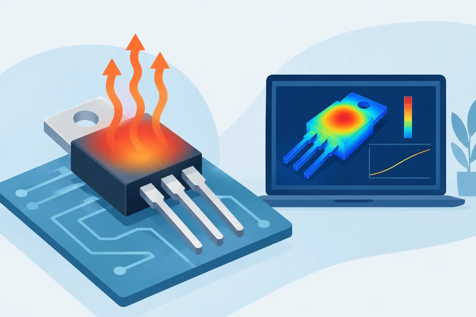
    A transistor self heating guide starts with a practical observation: the electrical operating point and the thermal operating point are not independent. A device that appears acceptable under isothermal assumptions can shift threshold voltage, mobility, saturation current, leakage, and reliability margin once internally generated heat is allowed to alter the local lattice temperature. For power transistors, RF structures, densely packed logic, and devices with poor heat removal paths, that difference can determine whether a design is usable.

    Self heating is therefore an electrothermal problem, not simply a post-processing temperature calculation. The current distribution establishes power dissipation. The resulting temperature field changes material properties and carrier transport. Those changes modify the current distribution and power again. A credible model must close that feedback loop with appropriate geometry, physical parameters, boundary conditions, and numerical controls.

    What transistor self heating actually represents

    In a semiconductor device, Joule heating is commonly represented by the local product of current density and electric field. Additional heat sources may arise from recombination, impact ionization, contact resistance, and energy relaxation mechanisms, depending on the transport model and device type. The heat equation then converts those sources into a spatial temperature distribution according to thermal conductivity, heat capacity for transient analysis, and heat flow through the surrounding structure.

    The critical point is locality. A reported average device temperature can conceal a narrow hotspot near a drain-side gate edge, current-crowded contact, field plate termination, or constricted interconnect. That hotspot may control degradation even when the package-level temperature estimate appears moderate. Mesh resolution, source-term placement, and material interfaces consequently matter as much as the nominal total power.

    For DC operation, the coupled solution seeks a steady state in which electrical power generation and heat removal balance. For pulsed operation, the thermal time constants of the active region, metallization, substrate, die attach, and package determine whether the device experiences a short-lived temperature spike or cumulative heating. A pulse width that is electrically brief may still be thermally significant if its repetition rate prevents adequate cooling.

    Define the question before selecting the model

    The necessary model complexity depends on the engineering decision. If the question is whether a modest bias shift changes channel temperature by a few degrees, a two-dimensional device cross-section with calibrated thermal boundaries may be sufficient. If the question concerns finger-to-finger temperature variation, via placement, substrate spreading, or a localized metallization bottleneck, a three-dimensional thermal model is generally required.

    Start by defining the quantity to be trusted. It may be peak channel temperature, thermal resistance from hotspot to ambient, temperature-dependent drain current, a safe-operating-area limit, or the transient temperature response to a power pulse. This choice determines the geometry and physics that cannot be omitted.

    A useful separation is between device-scale electrothermal coupling and structure-scale heat spreading. Device simulation resolves carrier transport, electric field, and heat generation in the active semiconductor. A larger thermal calculation resolves lateral spreading through the die, interconnect stack, package, heat sink, or neighboring heat sources. Combining every feature in one model is not automatically more accurate. It can introduce uncertain inputs and impractical mesh sizes. Use the model that resolves the mechanism controlling the result.

    Build the electrical model before coupling temperature

    An electrothermal calculation cannot correct an uncalibrated electrical model. Establish the isothermal device behavior first at relevant temperatures. Verify geometry, doping profiles, contacts, mobility, recombination, high-field transport, and any material-specific parameters against measured or otherwise credible reference data.

    Temperature dependence must be physically consistent. Mobility commonly declines as lattice temperature rises, but the magnitude and functional form depend on scattering mechanisms and doping. Bandgap narrowing, intrinsic carrier concentration, saturation velocity, contact behavior, and thermal conductivity may also vary strongly with temperature. In wide-bandgap devices, high electric fields and substrate thermal properties can make these dependencies particularly consequential.

    Do not treat thermal conductivity as a universal constant unless the anticipated temperature range justifies it. Silicon, silicon carbide, gallium nitride, metals, dielectrics, and interface layers can have very different temperature behavior. A constant value may be acceptable for an early comparison study, but it should be identified as an assumption rather than presented as a material prediction.

    Represent heat sources where they occur

    The simplest power estimate, terminal voltage multiplied by terminal current, is useful for a global energy check. It is not enough to locate a hotspot. The simulation should distribute heat generation according to the electrical solution, particularly in regions of high field or current crowding.

    Check that the volume integral of modeled heat generation is consistent with net electrical power entering the device, subject to stored energy and boundary flux in transient cases. This energy-balance check catches sign errors, incomplete source terms, and contact definitions that can otherwise produce plausible-looking but incorrect temperature contours.

    Thermal boundaries decide the result

    A thermal model is only as defensible as its heat-removal path. Fixed-temperature boundaries are appropriate where a region is genuinely held near a known temperature, such as an idealized heat spreader reference plane. They are often overused at the backside of a thin substrate, where die attach, solder, carrier, and cooling hardware add substantial thermal resistance.

    Convective boundaries require a realistic heat-transfer coefficient and ambient temperature. These values vary with airflow, surface orientation, enclosure geometry, and whether the device is attached to a heat sink. Radiation may be relevant at elevated temperatures or for exposed surfaces, but it rarely replaces a careful conduction model in packaged semiconductor assemblies.

    Thermal boundary resistance at material interfaces deserves explicit attention. Perfect thermal contact between semiconductor, oxide, metal, solder, and ceramic layers can materially understate peak temperature. Conversely, assigning a large interface resistance without measurement or literature support can dominate the result for the wrong reason. Sensitivity analysis is the appropriate response when interface data are uncertain.

    For early-stage work, state a range for uncertain boundary parameters and report the corresponding range of peak temperatures. A result such as 165 to 205 degrees C under credible interface assumptions is more useful than an unsupported prediction of 178 degrees C.

    Mesh for gradients, not visual smoothness

    Thermal gradients are usually sharp near localized heat sources, thin films, narrow contacts, and interfaces with large conductivity contrast. Refine the mesh in those areas and along the expected heat-flow path. A uniformly fine mesh can consume computation without improving the quantity of interest, while a coarse hotspot region can suppress the peak temperature and distort electrothermal feedback.

    Perform a mesh-convergence study on at least the outputs that drive the decision: maximum lattice temperature, total dissipated power, drain current, and thermal resistance. Refine the mesh until further refinement produces an acceptably small change. The acceptable change depends on the task. A research study may require tighter control than an engineering screening calculation, but neither should rely on a single untested mesh.

    For three-dimensional structures, mesh growth must be managed deliberately. SibLin is suited to thermal and related field calculations where spreading resistance, layered materials, and complex heat-flow paths require a numerical solution across large meshes. The value of a million-node capability is not the node count itself. It is the ability to place resolution at the hotspot and interfaces while retaining the full geometry needed to represent realistic heat removal.

    Solve electrothermal feedback carefully

    Fully coupled solutions can become difficult near strong nonlinearities. As temperature rises, reduced mobility may lower current under voltage bias and create negative feedback. In other conditions, leakage and temperature-dependent conduction can increase power and create positive feedback. The stability of the physical device and the stability of the numerical iteration are separate questions, although both must be examined.

    A practical approach is to ramp bias or dissipated power gradually from a known low-power solution. Use temperature limits and residual checks to identify whether a calculation is converging toward a physical steady state or merely oscillating between inconsistent electrical and thermal states. Under current-controlled and voltage-controlled conditions, the same device may exhibit substantially different feedback behavior, so the external bias condition must match the intended application.

    Transient simulation is necessary when the thermal time history affects performance or damage risk. Use time steps small enough to resolve fast electrical changes and early local heating, then allow larger steps as the response approaches slower package-scale thermal dynamics. Check time-step convergence just as carefully as spatial mesh convergence.

    Report results that can be reviewed

    A useful self-heating result includes more than a color temperature plot. Report the bias condition, ambient or reference temperature, electrical power, peak temperature and its location, boundary conditions, material thermal properties, interface assumptions, mesh-convergence evidence, and whether the solution is steady-state or transient. If possible, compare temperature-sensitive electrical characteristics with measurements, such as output-current roll-off, on-resistance shift, threshold shift, or pulsed versus DC behavior.

    The most productive next step is usually not a larger model. It is an uncertainty-focused one: identify whether the prediction is limited by heat-source physics, interface resistance, boundary conditions, or insufficient spatial resolution, then improve that part of the model first.

  • Chiplet Thermal Design: What Must Be Modeled

    Chiplet Thermal Design: What Must Be Modeled

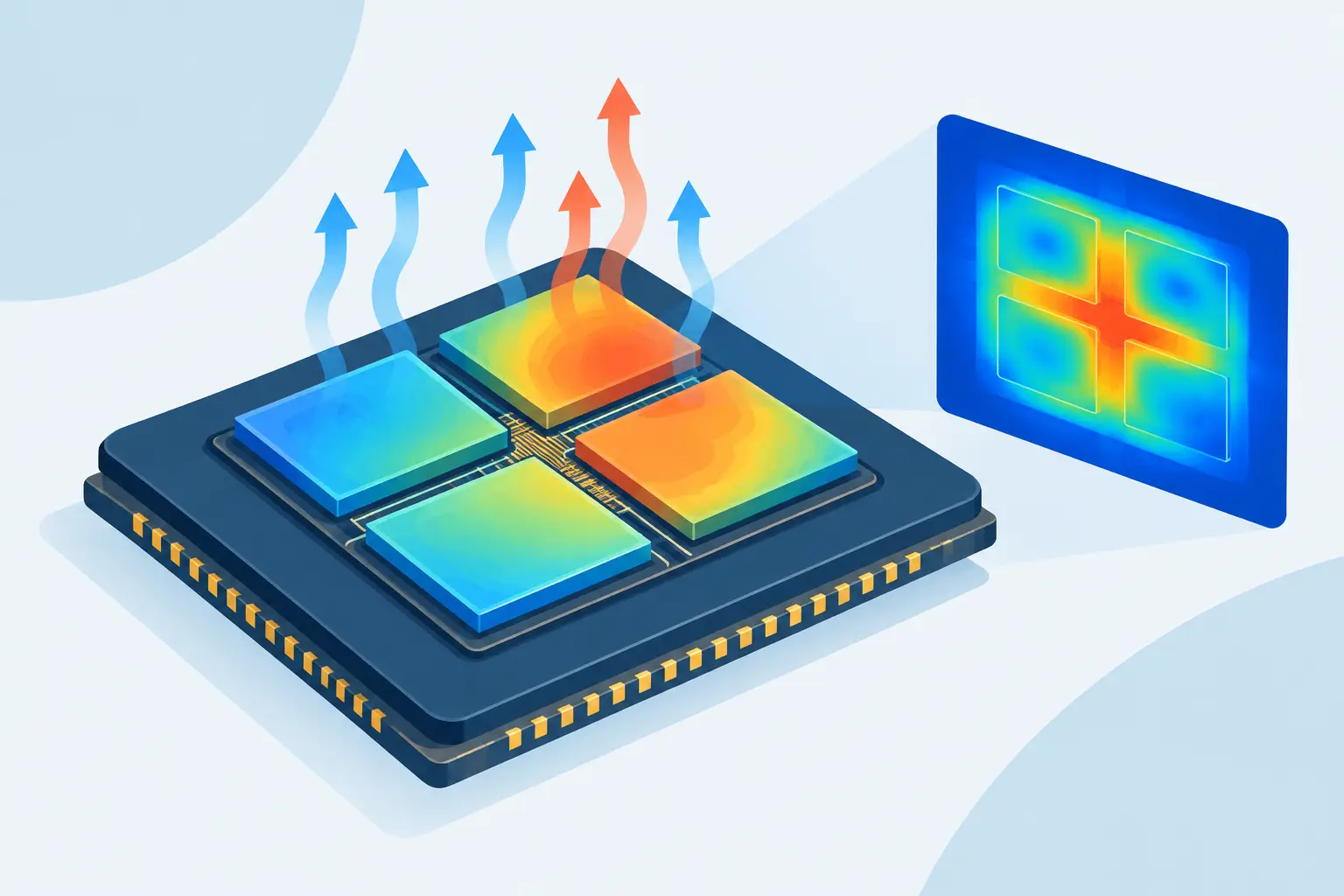
    A chiplet assembly can meet its electrical targets and still fail its operating envelope because its thermal path was treated as a package afterthought. In chiplet thermal design, heat is generated in spatially separate dies, crosses several thin and dissimilar interfaces, and is removed through a package whose geometry is rarely uniform. The relevant question is not simply whether total package power is acceptable. It is whether each chiplet, interface, and local interconnect region remains within temperature limits under the workload that produces the highest local dissipation.

    Why chiplet assemblies change the thermal problem

    A monolithic die has a continuous silicon heat-spreading layer, even if its power density is highly nonuniform. A chiplet-based system divides that layer into separate thermal sources. Compute chiplets, I/O dies, high-bandwidth memory stacks, analog functions, and cache dies may have different thicknesses, footprints, activity factors, and allowable junction temperatures. Their placement establishes thermal coupling before any cooling hardware is selected.

    The package adds further complexity. In a 2.5D configuration, heat may spread through microbumps, underfill, an interposer, substrate layers, a lid, thermal interface material, and a heat sink. In a 3D stack, vertical proximity can place a warm logic die beneath a memory die with a lower temperature limit. The effective thermal resistance of the assembly is therefore not a single material property or a single junction-to-ambient value. It is a three-dimensional conduction problem shaped by geometry, material interfaces, and boundary conditions.

    Chiplet partitioning also separates electrical and thermal decisions that were formerly made together. Moving an I/O function off a compute die may reduce compute-die power density but can add power sources at the package periphery. Enlarging a chiplet can improve lateral spreading within that die while changing placement options and bump-field density. A thermal model must be available early enough to assess these trade-offs, not only after floorplanning and package selection are fixed.

    Chiplet thermal design begins with the correct physical model

    The appropriate model depends on the decision being made. Early architecture work may begin with compact representations of each die, assigned power maps, and approximate package layers. That level can expose obvious placement problems, such as placing two peak-power chiplets beneath the same region of the lid. It cannot reliably resolve microbump crowding, narrow bridge structures, or localized hot spots near interfaces.

    Detailed analysis requires a three-dimensional representation of the heat path. At minimum, it should include the individual chiplet geometries, active and passive silicon regions where relevant, bump and underfill layers, interposer or bridge structures, package substrate, lid, thermal interface material, and the cooling boundary. Omission is reasonable only when the omitted region has a demonstrably small effect on the result being used for design.

    Material properties require the same discipline. Thermal conductivity is often temperature-dependent, and effective conductivity in composite layers is not necessarily the bulk value of any constituent. Underfill and dielectric layers can dominate local vertical resistance despite their small thickness. An interposer may spread heat effectively in one direction while its surrounding dielectric structure limits another path. Treating all layers as isotropic slabs can be useful for a first estimate, but it should not be mistaken for a resolved package model.

    Power maps are model inputs, not fixed labels

    A chiplet power number is insufficient for hot-spot analysis. The model needs a spatial distribution and a workload definition. A compute die may have a sustained average condition, a short boost condition, and a localized accelerator workload that generate materially different temperature fields. Memory traffic can change both the memory stack dissipation and the power generated in neighboring logic.

    Power should also be updated when temperature affects leakage or electrical resistance. For some designs, a one-way calculation from power map to temperature is adequate. For high-leakage logic, dense power delivery structures, or temperature-sensitive interconnect resistance, electrothermal iteration is more credible: solve temperature, update temperature-dependent power or material behavior, and repeat until the solution is consistent.

    Interface resistance deserves explicit treatment

    The largest temperature gradients are often not inside a silicon chiplet. They occur across thin interfaces. Microbump arrays, underfill, die attach, thermal interface material, and lid contact conditions each introduce resistance that may vary by location and process quality.

    A model that replaces a bump field with a uniform layer may be appropriate for package-scale temperature trends. It is less appropriate when assessing a small high-power block above a nonuniform bump distribution. The correct level of detail depends on whether the engineering decision concerns die placement, local reliability, bump-current interaction, or heat-sink selection. Use the simplest representation that preserves the thermal gradient relevant to that decision.

    Mesh resolution must follow the gradient

    A million-node three-dimensional model is not automatically more useful than a smaller one. Thermal simulation quality depends on whether the mesh resolves the regions in which geometry or material changes drive the result. Thin thermal interface layers, chiplet edges, bump fields, narrow interposer bridges, and localized heat sources need local refinement. Large uniform regions can generally use a coarser mesh.

    Mesh convergence should be checked against the quantities that matter: maximum junction temperature, temperature at specified sensor locations, temperature difference between neighboring chiplets, and gradients across critical interfaces. If a modest refinement changes a reported hot-spot temperature substantially, the model is not yet ready to support a margin decision.

    The solver also matters. Chiplet packages combine high-conductivity silicon and metals with much lower-conductivity dielectrics and polymers. This contrast, together with thin layers and large aspect ratios, can produce poorly conditioned numerical systems. Reliable results require numerical methods that handle heterogeneous material domains and large three-dimensional meshes without disguising nonconvergence as a physical result. Siborg’s SibLin v1.2 is designed for this class of three-dimensional heat-transfer problem and can solve meshes exceeding 1,000,000 nodes when the geometry requires that resolution.

    Boundary conditions can dominate the result

    The heat sink is not a constant-temperature surface in normal operation. Its effectiveness depends on heat-sink geometry, airflow or liquid flow, mounting pressure, thermal interface behavior, and the temperature of the surrounding environment. A fixed-temperature boundary may be valid for comparing internal package alternatives, but it can understate the junction temperature obtained in a complete system.

    Convection boundaries require justified heat-transfer coefficients and ambient temperatures. These values may differ across a heat sink and may change with orientation, fan speed, neighboring components, or recirculated air. For liquid-cooled systems, coolant temperature rise along the flow path can matter. For mobile systems, transient enclosure heating can be more consequential than steady-state ambient conditions.

    Radiation is usually secondary within a tightly coupled package heat path, though it may matter at exposed system surfaces. Contact resistance, by contrast, should rarely be dismissed without evidence. A nominally thin interface can produce a significant temperature rise when its effective area is restricted or its bond quality varies.

    Steady state is necessary, but transient behavior may decide the design

    Steady-state simulation establishes the sustained thermal limit. It does not explain whether a short workload burst produces an unacceptable local temperature excursion, whether a control loop responds quickly enough, or how one chiplet heats another after a delay. Thermal capacitance in silicon, lids, and heat sinks creates time constants that vary widely across the assembly.

    Transient analysis is particularly useful when power management is part of the thermal strategy. A controller may safely permit a brief power increase if the local thermal time constant is long enough and sensor placement captures the relevant hot spot. Conversely, a sensor located far from a fast local heat source may report an acceptable temperature while a nearby region exceeds its limit. The model should represent the duration and sequence of real workloads, not merely an arbitrary step in total package power.

    A practical simulation sequence

    Start with an architectural model that compares chiplet placement and broad cooling concepts using representative power maps. Then introduce package geometry and interfaces as the design becomes defined. Before release, use a resolved model to evaluate worst-case power distributions, material tolerances, mounting conditions, and cooling boundaries.

    Do not treat the resulting maximum temperature as a single definitive number. Report the assumptions that produced it: die powers, activity profiles, material data, interface resistances, ambient condition, convection model, and mesh-convergence result. This makes the analysis reviewable and shows which uncertainty deserves measurement or design margin.

    Thermal design is most effective when it changes a decision while that decision is still inexpensive. If a chiplet location, bump-field layout, lid thickness, or cooling requirement looks marginal in simulation, revise it before the package geometry turns a correctable gradient into a qualification problem.

  • Junction Depth in Semiconductor Process Control

    Junction Depth in Semiconductor Process Control

    A junction that is only a few tens of nanometers deeper or shallower than intended can shift a device from acceptable performance to excessive leakage, premature breakdown, or an unworkable resistance target. Junction depth is therefore not a reporting detail after diffusion or implantation. It is a process and device-design variable that must be defined consistently, measured carefully, and evaluated against the complete dopant profile.

    For process engineers, the useful question is rarely simply, “What is the junction depth?” The more useful questions are: at which concentration is it defined, how does it vary across the wafer, what is the lateral extent beneath critical edges, and how does it affect the electrical behavior of the finished structure? Those questions connect process conditions directly to device operation.

    What Junction Depth Actually Represents

    In the conventional process sense, junction depth, often written as xj, is the vertical location at which an introduced dopant concentration equals the background concentration of the substrate or well. At that crossing point, the material changes conductivity type. An n-type dopant profile introduced into a p-type substrate forms a p-n junction where the donor and acceptor concentrations balance.

    This metallurgical definition is indispensable, but it is not the only definition that matters. Electrical junction behavior depends on the net active dopant distribution, compensation, incomplete ionization where applicable, defect-related leakage, and the local electric field. A chemical dopant profile measured by a technique such as secondary-ion mass spectrometry may not match the electrically active profile after implant damage, clustering, transient enhanced diffusion, or incomplete anneal activation are considered.

    The distinction becomes particularly relevant in shallow junction technologies. When the gradient is steep, a small uncertainty in concentration or activation can move the apparent crossing point substantially. Reporting xj without the concentration profile, substrate doping, and definition used can obscure the process information an engineer needs to reproduce the result.

    Vertical and Lateral Junction Extent

    The vertical junction depth is only part of the geometry. Diffusion and post-implant annealing also move dopants laterally, especially beneath mask edges, gate structures, field oxide edges, and contact openings. Lateral diffusion can alter overlap capacitance, effective channel length, source-drain separation, and edge electric fields even when the vertical xj meets specification.

    For this reason, a one-dimensional profile is often adequate for early diffusion studies, but not for structures in which neighboring regions, masks, or surface boundaries influence device behavior. A two-dimensional process model provides the geometry needed to evaluate both vertical penetration and lateral encroachment before a wafer split is committed.

    Why Junction Depth Drives Device Trade-Offs

    A shallow junction generally reduces the volume of doped material and can support tighter device dimensions. It may reduce short-channel effects in scaled MOS structures when combined with an appropriate channel and extension design. But shallower is not automatically better. Sheet resistance rises as the conducting layer becomes thinner, and the resistance can become highly sensitive to activation and dose variation.

    A deeper junction can lower series resistance and provide a larger conducting cross-section. It can also increase junction capacitance, enlarge lateral diffusion, and alter the depletion-region geometry. In power or high-voltage devices, junction placement affects peak electric field and breakdown behavior. In analog and RF structures, the associated capacitance and parasitic resistance may set bandwidth or noise limits.

    The central trade-off is profile shape, not depth alone. Two profiles with the same xj can have different peak concentrations, gradients, sheet resistances, and depletion widths. A high-dose, abrupt profile may satisfy a shallow-depth target while creating leakage or defect concerns. A deeper, graded profile may have a comparable sheet resistance but produce a different electric-field distribution.

    Process specifications should therefore pair junction depth with quantities that describe the profile’s electrical consequence. Common companions include sheet resistance, surface concentration, dose, activation fraction, leakage current, breakdown voltage, and lateral diffusion. The appropriate set depends on the device. A bipolar emitter, a CMOS source-drain extension, a photodiode, and a high-voltage diffusion should not be controlled by the same limited metric set.

    Process Variables That Set Junction Depth

    For thermal diffusion, junction depth is determined by the dopant source condition, diffusion coefficient, thermal budget, ambient, and starting substrate concentration. Predeposition establishes a near-surface dopant supply; drive-in redistributes that dose more deeply. Temperature has an especially strong effect because diffusion coefficients vary exponentially with temperature. A modest furnace-temperature shift or an unaccounted thermal step can materially change xj.

    Ion implantation introduces a different set of controls. Implant energy establishes the initial projected range, while dose sets the total dopant quantity. Tilt, rotation, crystal orientation, screen oxides, and channeling control the as-implanted distribution. Subsequent annealing activates dopants and repairs damage, but it also changes the profile through ordinary diffusion and, in some materials and conditions, transient enhanced diffusion.

    Four interactions routinely complicate process control:

    • Implant energy and screen-layer thickness determine how deeply the as-implanted distribution begins.
    • Anneal temperature, duration, and ramp rate determine activation and redistribution together.
    • Background well or substrate concentration changes the metallurgical crossing point even if the introduced profile is unchanged.
    • Mask geometry and neighboring regions influence lateral diffusion and local thermal behavior.

    These interactions explain why a target xj cannot be transferred blindly between device platforms. A diffusion recipe that is satisfactory in a lightly doped substrate can yield a substantially different metallurgical depth in a higher-doped well. Likewise, an implant condition that produces the expected one-dimensional profile may behave differently near a gate edge or isolation boundary.

    Modeling the Junction Before Fabrication

    Physical simulation is most useful when it preserves the connection between the process sequence and the resulting electrical structure. Rather than treating junction depth as an isolated output, the model should track dopant introduction, diffusion, activation assumptions, geometry, and the net doping distribution used by the device calculation.

    A practical workflow begins with the actual starting structure: substrate or well concentration, relevant oxide layers, and mask geometry. The process sequence should then include each thermal exposure that contributes materially to redistribution, not only the nominal drive-in or activation anneal. Later oxidation, contact anneals, and epitaxial steps can contribute enough thermal budget to matter in shallow-profile work.

    The resulting profile should be inspected at more than one location. A vertical cut through the center of a diffusion region can establish nominal xj, while cuts near edges reveal lateral encroachment and curvature of the junction. Contour plots of net doping are often more informative than a single reported depth because they expose whether the junction is planar, rounded, pinched, or influenced by an adjacent region.

    MicroTec is suited to this class of two-dimensional semiconductor process and device analysis, where initial diffusion profiles, process steps, and resulting device behavior need to be evaluated in the same engineering workflow. The objective is not to replace measurement. It is to reduce the number of wafer experiments required to identify a credible process window and to clarify which variable is responsible when measured results shift.

    Correlating Simulation With Measurement

    No profile model should be accepted solely because it produces a plausible xj. Calibration requires comparison with measurements that are sensitive to both depth and electrical activity. Sheet resistance is a useful integrated electrical constraint, but it cannot uniquely establish the profile shape. Capacitance-voltage analysis can indicate electrically active junction behavior and depletion characteristics. Spreading-resistance profiling, electrochemical capacitance-voltage profiling, and secondary-ion mass spectrometry each provide different information and have different depth-resolution and interpretation limits.

    The strongest correlation usually combines at least one chemical profile measurement with one electrical measurement. If SIMS indicates the expected total dose but sheet resistance is too high, incomplete activation or excessive redistribution may be involved. If sheet resistance agrees but leakage is excessive, the explanation may lie in defects, junction curvature, surface effects, or local electric-field concentration rather than nominal xj.

    Process teams should also account for the definition used by each method. A junction inferred from net electrically active concentration will not necessarily coincide with one inferred from total chemical concentration. Consistent definitions are essential when comparing historical data, simulation output, and in-line metrology.

    Setting a Useful Process Window

    A defensible junction-depth specification states more than a nominal value and tolerance. It identifies the structure location, the depth definition, the background concentration or well condition, and the associated electrical constraints. For example, a shallow source-drain target may require a specified xj range together with sheet resistance and leakage limits, while a high-voltage diffusion may require xj, lateral extent, and breakdown-voltage verification.

    Sensitivity analysis is valuable before setting those limits. Vary implant energy, dose, anneal conditions, and starting concentration within realistic manufacturing ranges, then observe which variables move the junction most strongly. The result distinguishes a process that is nominally correct from one that remains acceptable under expected equipment and material variation.

    That distinction is where junction-depth analysis earns its place in process development. A number on a profile plot is useful; a controlled relationship between thermal budget, geometry, dopant distribution, and electrical performance is what supports a manufacturable device.

  • Thermal Solvers for Electronics: What Matters

    Thermal Solvers for Electronics: What Matters

    A temperature map is only useful if it explains the engineering decision in front of you. For a device engineer, that may mean locating a localized hot spot before it changes mobility or accelerates degradation. For a package or interconnect researcher, it may mean separating a genuine spreading-resistance effect from an artifact of mesh design. Thermal solvers are the numerical engine behind those decisions, but their value depends on how well their physics, geometry, boundary conditions, and numerical method match the problem.

    What thermal solvers actually solve

    At their core, thermal solvers calculate the temperature field in a structure by enforcing conservation of energy. In steady-state form, the governing equation is commonly written as:

    `∇ · (k∇T) + Q = 0`

    Here, `T` is temperature, `k` is thermal conductivity, and `Q` represents volumetric heat generation. Transient analysis adds heat storage through density and specific heat. The equation is compact; the engineering problem is not. Conductivity may vary by material, temperature, crystal orientation, or layer. Heat generation may be concentrated in a small active region. Interfaces, contacts, convection boundaries, and fixed-temperature surfaces can dominate the result.

    A useful solver does more than produce a colored contour plot. It should resolve gradients where the physics demands resolution, preserve numerical stability on practical meshes, and allow the engineer to test whether the result changes when assumptions are refined. The relevant question is not whether a solver can calculate temperature. Nearly every thermal code can do that for a simple block. The question is whether it can calculate the right temperature distribution for the actual electronic structure under study.

    Why electronic thermal problems are rarely simple

    Semiconductor and electronic assemblies combine sharply different length scales. A heat-generating region may be measured in microns, while the substrate, package, heat spreader, or surrounding domain is orders of magnitude larger. A mesh that is sufficiently fine everywhere can become prohibitively expensive. A mesh that is too coarse near a source, interface, or narrow current path can flatten the very gradient that determines the design outcome.

    Material contrast creates another difficulty. Silicon, dielectrics, metals, adhesives, and ambient regions conduct heat differently. In thin multilayer structures, thermal resistance may be governed less by the bulk material than by a poorly represented interface or an assumed boundary condition. Treating a contact as perfectly isothermal, for example, can make a predicted peak temperature look reassuringly low while concealing a bottleneck in the real structure.

    Heat is also coupled to other device behavior. Joule heating depends on current distribution. Carrier transport and mobility can change with temperature. In power devices, electrothermal feedback may concentrate dissipation where the local temperature has already risen. In these cases, a thermal solution is not necessarily the end of the analysis. It may need to be coupled to Poisson, diffusion, drift-current, or spreading-resistance equations.

    Selecting thermal solvers by problem dimension

    The first selection decision is usually dimensionality. A two-dimensional thermal model is appropriate when the geometry and heat flow are effectively invariant along one axis, or when it is being used early in device development to examine cross-sectional behavior. It can be fast, transparent, and highly useful for comparing process or layout alternatives.

    A three-dimensional model is required when lateral heat spreading, finite contact geometry, nonuniform sources, or asymmetric boundary conditions determine the result. This is common in real packages, resistor networks, sensor structures, power devices, and layered electronic assemblies. A 2D model may estimate vertical heat flow correctly yet miss a lateral path that either relieves or intensifies a local hot spot.

    Neither approach is inherently superior. The practical choice depends on what must be resolved. Starting in 2D is often sensible when establishing material parameters, source profiles, and boundary assumptions. Moving to 3D becomes necessary when the omitted dimension changes the resistance network or local temperature maximum. Engineers should avoid treating a lower-dimensional model as a final answer simply because it runs quickly, but they should also avoid using a large 3D mesh where a validated 2D representation answers the question directly.

    Mesh capacity is not the same as mesh quality

    Large problems require large meshes, but node count alone does not establish credibility. A million-node model can still be wrong if critical interfaces are under-resolved or if the outer boundary is placed too close to the heat source. Conversely, a smaller mesh can provide an excellent answer when it is concentrated around steep gradients and paired with physically justified boundaries.

    Mesh-convergence testing remains one of the most effective checks. Refine the regions around active devices, narrow conductors, material transitions, and peak-temperature locations. Then compare the quantities that drive the decision: maximum temperature, temperature difference across an interface, heat flux through a boundary, or equivalent thermal resistance. If those quantities move materially with refinement, the model has not yet earned confidence.

    The numerical formulation matters as well. Thermal solvers should remain stable across irregular geometries and substantial conductivity variation, without forcing the user into excessive manual tuning. For research and industrial design work, the preferred tool is one that can solve the required mesh while leaving time for sensitivity studies. A single expensive run is less valuable than a workflow that permits engineers to test the assumptions behind it.

    Boundary conditions deserve the same scrutiny as equations

    Many thermal simulations fail quietly at the boundary. A fixed-temperature boundary is convenient, but it represents a perfect heat sink at a prescribed location. Convection conditions require a heat-transfer coefficient and ambient temperature, both of which may be uncertain. Adiabatic boundaries can be appropriate at planes of symmetry, but not as a default method for reducing model size.

    The boundary should represent the physical test or operating environment. If a device is mounted to a temperature-controlled chuck, a fixed-temperature boundary may be justified at the chuck interface. If heat leaves through air or liquid cooling, convection and radiation may need consideration. If the model terminates within a substrate or package, the analyst should establish that the truncation boundary is far enough away not to distort the thermal field.

    A disciplined approach is to run sensitivity cases. Vary the convection coefficient, interface resistance, source power, or sink temperature within credible ranges. The resulting spread in peak temperature may be more useful to a design review than a single value reported to an unrealistic number of decimal places.

    Coupled physics changes the tool requirement

    A thermal-only calculation is suitable when power dissipation is known and does not change appreciably with temperature. That assumption is often reasonable for a prescribed resistor, a fixed heat source, or an initial package study. It becomes weaker when current crowding, temperature-dependent conductivity, or semiconductor transport affects where power is generated.

    For coupled problems, the solver must support a consistent treatment of the relevant equations and variables. Heat generation should arise from the electrical solution where appropriate, and temperature should feed back into material parameters when the physics requires it. This adds computational cost and modeling responsibility, but it can be essential for predicting hot spots, failure margins, and nonuniform device behavior.

    This is also where standalone tools can be advantageous. An engineer investigating a 3D heat-transfer or spreading-resistance problem does not necessarily need a broad software suite designed for unrelated workflows. Siborg Systems’ SibLin, for example, is designed for three-dimensional numerical problems involving heat transfer alongside Poisson, diffusion, drift-current, and spreading-resistance equations, including meshes exceeding 1,000,000 nodes. The appropriate choice remains problem-specific: select the simulator that matches the governing physics and geometry, not a bundle that adds complexity without analytical value.

    A practical verification sequence

    Before accepting a thermal result, establish the intended use of the model. Is it screening alternatives, correlating with measurement, estimating a safe operating limit, or supplying temperature data to an electrical calculation? The required level of geometric detail follows from that purpose.

    Next, check energy balance. The heat entering or generated within the domain should be consistent with heat leaving through its boundaries, within the expected numerical tolerance. Review the temperature field for nonphysical discontinuities, unexpected extrema, and gradients that align suspiciously with coarse mesh transitions rather than material features.

    Then compare against an independent reference whenever one exists. This may be an analytical resistance estimate, a simplified one-dimensional calculation, a measured thermal resistance, or a known limiting case. Agreement does not prove every model assumption, but disagreement often identifies where the model needs attention.

    Finally, document the inputs that matter: material properties, source definition, interface treatment, boundary conditions, mesh strategy, convergence behavior, and sensitivity results. Thermal simulation becomes much more valuable when another engineer can understand why the result is credible and what operating range it supports.

    A well-chosen thermal model should leave the engineering team with a decision they can defend: where heat is generated, how it escapes, which assumption controls the uncertainty, and what design change is most likely to improve the result.

  • TCAD Alternatives: Choose the Right Solver

    TCAD Alternatives: Choose the Right Solver

    A TCAD evaluation often begins after a practical constraint appears: the available simulator is too broad, too difficult to deploy, poorly matched to a two-dimensional device study, or unable to solve the thermal or electrical field problem that is actually limiting the design. The useful question is not which platform has the longest feature list. It is which TCAD alternatives solve the governing equations, geometry, and workflow of the engineering problem with sufficient numerical reliability.

    For semiconductor engineers and researchers, this distinction affects both project time and confidence in the result. A process diffusion study, a p-n junction analysis, a three-dimensional heat-flow model, and a spreading-resistance calculation may all be described as TCAD work. They do not necessarily require the same software architecture, mesh capability, licensing model, or level of physical detail.

    Start with the physics, not the software category

    The term TCAD covers a wide range of simulation tasks. Process simulation may require dopant diffusion, oxidation, implantation profiles, and subsequent geometry changes. Device simulation commonly combines Poisson and carrier continuity equations with drift-diffusion transport, recombination models, and material parameters. Thermal and field analysis may instead center on heat transfer, electrostatics, diffusion, or current flow across a three-dimensional structure.

    A suitable tool should make the primary equations explicit. If the problem is a two-dimensional semiconductor process or device model, a dedicated 2D process and device simulator may be more appropriate than a large multiphysics environment intended for many unrelated disciplines. If the limiting question is temperature distribution through a package, substrate, or complex electronic assembly, a 3D numerical field solver may be the better fit.

    This is not an argument against broad simulation suites. They are appropriate when a team must couple several physical domains, share models across departments, or standardize on one enterprise environment. The trade-off is often configuration overhead, higher licensing cost, and a workflow designed for users who spend most of their time administering a simulation platform. For a focused engineering study, those costs may not improve the answer.

    TCAD alternatives should match dimensionality

    Dimensionality is one of the first decisions in a credible evaluation. A two-dimensional model is not merely a smaller three-dimensional model. It is an assumption about the device structure, symmetry, current paths, and the degree to which out-of-plane effects can be neglected.

    For planar devices, diffusion-profile development, teaching examples, and many cross-sectional process studies, 2D simulation can provide useful physical insight with substantially lower computational cost. It also enables rapid parameter studies, where the engineer needs to examine the effect of junction depth, dose, oxide thickness, or bias conditions over many runs.

    Three-dimensional analysis becomes necessary when the structure itself is inherently 3D. Examples include localized heat sources, nonuniform package interfaces, irregular conductor paths, multi-contact current spreading, and geometries where a cross-section conceals the dominant resistance or thermal path. In these cases, an apparently sophisticated 2D result can be less useful than a carefully constructed 3D model with the appropriate boundary conditions.

    Mesh scale matters as much as nominal 3D support. A solver intended for serious thermal or electrical-field work should state its practical capacity and numerical method. Models with 1,000,000+ mesh nodes demand more than memory alone. They require stable matrix handling, suitable discretization, convergence control, and a workflow that lets the engineer inspect whether the mesh is resolving the gradients that matter.

    When 2D remains the better engineering choice

    A 2D model is often the right choice when the objective is to establish a device profile, compare process variations, analyze a planar cross-section, or teach the relationship between fabrication steps and electrical behavior. The value lies in iteration speed and physical transparency. Adding a third dimension without evidence that it changes the result can obscure the model rather than improve it.

    The limitation is equally clear: 2D cannot represent lateral heat escape, finite contact layouts, or nonuniform current crowding in the omitted direction. Engineers should treat dimensionality as a model decision to validate, not as a product tier to purchase.

    Compare numerical methods before interface features

    A polished preprocessor and extensive material library are useful, but they do not substitute for numerical behavior. Semiconductor and field problems can be strongly nonlinear, stiff, and sensitive to boundary conditions. The solver must handle coupled equations without producing a result that appears converged while failing to represent the underlying physics adequately.

    For device work, assess how the software formulates and solves Poisson and carrier transport equations. Determine which mobility, recombination, and generation mechanisms are relevant to the operating regime. For process work, examine the available diffusion and oxidation formulations, grid handling, and the ability to translate process results into a device calculation. For heat and field analysis, verify support for the required heat-transfer, diffusion, drift-current, Poisson, and spreading-resistance equations.

    Ask practical questions during evaluation. Can material properties vary by region or temperature? Are boundary conditions defined in physical engineering terms? Can the user refine the mesh near junctions, interfaces, contacts, or concentrated heat sources? Does the software report residual behavior and provide enough diagnostic information to distinguish a difficult problem from an incorrect setup?

    No simulator can compensate for uncertain parameters or incomplete geometry. A technically sound workflow makes assumptions visible, permits controlled refinement, and supports comparison with measurement, analytical limits, or established benchmark structures.

    Evaluate the workflow your team will actually use

    Some TCAD products assume a dedicated simulation specialist who writes scripts, manages databases, and develops custom model libraries. That approach can be justified in high-volume development environments with complex, repeated flows. It may be excessive for a device engineer, university researcher, or thermal specialist who needs reliable results without maintaining an enterprise simulation stack.

    Standalone tools have a different advantage. They can reduce the path from physical problem to numerical model when the scope is well defined. A focused process and device simulator supports engineers establishing diffusion profiles and examining device behavior. A separate 3D solver can address heat transfer, potential distribution, diffusion, drift current, and spreading resistance without forcing those workloads into a single bundled environment.

    Siborg Systems follows this focused approach with MicroTec for two-dimensional semiconductor process and device modeling, and SibLin for three-dimensional numerical field problems. The distinction is useful because it reflects a real engineering choice: select the solver that corresponds to the model, rather than acquiring a suite whose unused modules add cost and complexity.

    Workflow evaluation should also include reproducibility. Teams need to save model assumptions, rerun cases after parameter changes, and communicate inputs and results to colleagues or reviewers. In academic settings, the same requirement supports instruction: students should be able to connect equations, material parameters, geometry, and output rather than treat simulation as a black box.

    Licensing and support are technical considerations

    Licensing is sometimes treated as a procurement detail, but it shapes engineering access. A tool that is difficult to license for an individual researcher, small R&D group, or teaching lab may remain underused regardless of its capabilities. Conversely, a low-cost tool with inadequate numerical scope can create false economy if it cannot represent the problem.

    Compare whether licensing is tied to a large suite, a network environment, a cloud service, or a standalone product. Consider how users will access the software, whether students or external collaborators need it, and how long model files must remain reproducible. Long-term projects benefit from stable tools and documentation that do not depend on a constantly changing online service.

    Technical support should be assessed with the same discipline. The relevant question is not simply response time. It is whether support personnel understand the equations, meshing decisions, and boundary-condition issues behind the reported result. For specialized semiconductor and numerical-field work, domain knowledge is often more valuable than generic software assistance.

    A disciplined selection process for TCAD alternatives

    The most effective evaluation is a representative benchmark, not a feature checklist. Build a test case with known geometry, material data, boundary conditions, and an expected trend from measurement or theory. Run it at more than one mesh density. Change a parameter that should affect the result. Inspect convergence behavior, output clarity, computation time, and the effort required to reproduce the model.

    Then evaluate the next problem the team expects to solve. A tool can perform well on a textbook diode while being unsuitable for a 3D thermal path or a spreading-resistance geometry. Two specialized tools may be a more rational investment than one large platform if each produces better results for its intended workload.

    The right simulator is the one that makes the governing physics inspectable, the numerical solution credible, and the engineering decision easier to defend. Start from the problem on the bench or in the process flow, then choose the solver that gives that problem the attention it requires.

  • Numerical Stability in Engineering Simulation

    Numerical Stability in Engineering Simulation

    A converged simulation can still be wrong. A semiconductor potential profile may look smooth, a thermal map may show plausible gradients, and a current-density plot may contain no obvious discontinuities – yet the result can be dominated by numerical error rather than the governing physics. Numerical stability is what separates a computed answer from an engineering result that can support a design decision.

    For semiconductor process, device, and three-dimensional field problems, stability is not a single solver setting. It is the combined behavior of the discretization, mesh, equation scaling, boundary conditions, material models, and nonlinear solution method. The practical question is direct: if the mesh is refined, the bias is stepped differently, or the initial condition changes, does the physical conclusion remain credible?

    What Numerical Stability Means in Practice

    A numerical method is stable when small perturbations do not grow without control as the calculation proceeds. Those perturbations may come from roundoff error, interpolation, a coarse mesh, imperfect initial guesses, or the finite precision of the computer. In an unstable calculation, small errors can amplify into oscillations, divergence, negative concentrations, nonphysical temperatures, or solution values that depend more on numerical choices than on the device under study.

    Stability is related to, but different from, convergence and accuracy. Convergence means an iterative method has met its stopping criterion. Accuracy means the computed solution is sufficiently close to the physical solution. A solver can converge accurately on a coarse region while missing a sharp junction, or converge to a mathematically valid branch that is not the intended operating state. Stability provides the conditions under which refinement and iteration lead toward a meaningful answer rather than away from it.

    This distinction matters in coupled semiconductor problems. Poisson’s equation, carrier transport, diffusion, and heat transfer may each be well understood in isolation. Once coupled through temperature-dependent mobility, high doping gradients, field-dependent transport, or self-heating, their scales and nonlinearities interact. A solution strategy that works for a low-field equilibrium calculation may fail under high bias or during a transient process step.

    Where Numerical Stability Is Lost

    The first common source is spatial discretization. Semiconductor structures frequently contain narrow depletion regions, steep dopant gradients, thin oxides, contact edges, and localized heat sources. If the mesh does not resolve the relevant length scale, the solver must represent a sharp physical change across too few elements. The result can be artificial oscillation, excessive numerical diffusion, or a peak field that is substantially underestimated.

    Refining every part of the model is not automatically the answer. A uniformly fine three-dimensional mesh can produce an unnecessarily large system and may expose poor equation scaling or an unsuitable iterative method. The better approach is targeted refinement where gradients, interfaces, current crowding, or geometry changes require it. Mesh transitions also matter. An abrupt jump from very small to very large elements can introduce interpolation error and degrade conditioning.

    Advection-dominated transport presents a related problem. When drift or directed flow overwhelms diffusion, a standard central discretization may create oscillatory concentration or carrier profiles. Upwind or exponentially fitted formulations can improve stability, but they introduce a trade-off. Too much numerical damping smears the feature that the calculation is intended to resolve. The appropriate formulation depends on the local transport regime, not on a universal preference for one scheme.

    Time stepping is another frequent cause. Explicit methods are attractive because each step can be comparatively simple, but their stable time step can be severely restricted by diffusion, fine mesh spacing, or thermal properties. Implicit methods allow larger steps, although they require nonlinear or linear systems to be solved at each step. A large implicit step may be stable in the narrow mathematical sense while still skipping important physical evolution. Stable does not mean adequately resolved in time.

    Boundary conditions deserve the same scrutiny as the interior equations. A contact assigned the wrong potential reference, an artificial thermal boundary placed too close to an active region, or an inappropriate symmetry condition can force a solution that looks well behaved but represents the wrong device. Numerical stability cannot compensate for an ill-posed physical model.

    Numerical Stability in Nonlinear Device Problems

    Nonlinear semiconductor equations require a solution path as well as a discretization. Newton-type methods can converge rapidly near the solution, but they may diverge when started too far away or when the Jacobian is poorly conditioned. Damping, continuation, and bias stepping are practical methods for keeping iterations within a region where linearization remains useful.

    Consider a device simulation moved from equilibrium to a high drain or collector bias. Applying the final bias in one increment may produce large carrier and potential changes that make the next Newton update unrealistic. Incremental bias stepping uses the converged lower-bias state as the initial estimate for the next state. Smaller increments near threshold, breakdown, strong injection, or self-heating often improve reliability because those are the regions where the solution changes most rapidly.

    The same principle applies to process simulations. Large temperature steps, abrupt changes in diffusivity, or poorly resolved initial concentration profiles can generate nonphysical concentration behavior. A calculation should preserve properties that the underlying physics requires, such as nonnegative concentrations and sensible conservation behavior. If these properties fail, reducing the nonlinear tolerance alone is rarely the right repair.

    Equation scaling is especially important when a model combines variables with very different magnitudes and units. Electrostatic potential, carrier density, temperature, heat flux, and current density can differ by many orders of magnitude. Without appropriate scaling, a linear solver may treat one residual as dominant while effectively ignoring another. Reported convergence then becomes difficult to interpret. Residuals should be assessed in physically meaningful normalized terms, alongside changes in quantities that matter to the design.

    A Practical Verification Workflow

    Reliable simulation work benefits from a disciplined sequence rather than a search for a single ideal setting. Start with a model simple enough to check: known material parameters, clear boundaries, and a mesh that resolves the expected critical regions. Confirm that equilibrium or a low-stress operating condition behaves as expected before adding high bias, complex geometry, temperature coupling, or transient effects.

    Then test mesh dependence. Refine the mesh near junctions, interfaces, contacts, and localized heat sources, and compare the quantities used to make decisions. Peak electric field may be mesh-sensitive even when terminal current is not. A thermal resistance may appear converged while the local maximum temperature still changes materially. The relevant metric depends on the engineering question.

    Solver tolerances should be tightened only after the model has reasonable resolution. Extremely tight tolerances on a coarse mesh produce a very precise solution to an inadequately represented geometry. Conversely, a fine mesh with loose linear-solver tolerances can leave iteration error large enough to obscure the benefit of refinement. Compare terminal quantities, local extrema, conservation checks, and residual histories together.

    For nonlinear problems, repeat selected cases with altered initial guesses, bias increments, or time-step schedules. If materially different final states emerge under reasonable numerical changes, the result requires investigation. The explanation may be a genuine physical multistability, but it may also be a numerical branch-selection problem. Treating one converged run as proof is not sufficient.

    Choosing Tools That Expose the Problem

    A simulation environment should make numerical behavior inspectable rather than hiding it behind a convergence message. Engineers need access to mesh control, boundary-condition definition, solver settings, and output fields that reveal gradients and extrema. They also need methods suited to the equations being solved. A two-dimensional process and device calculation does not demand the same numerical machinery as a three-dimensional heat-transfer or spreading-resistance problem with more than 1,000,000 mesh nodes.

    This is why focused tools can be preferable to broad software bundles. MicroTec supports two-dimensional semiconductor process and device modeling, while SibLin addresses three-dimensional Poisson, diffusion, drift-current, heat-transfer, and spreading-resistance calculations. The relevant criterion is not the number of modules available. It is whether the formulation, mesh capacity, and solver behavior match the physical problem and permit credible verification.

    Numerical Stability Is an Engineering Check

    No solver setting can turn insufficient physical information into a reliable prediction. Material parameters must be valid over the temperature, doping, and field range of interest. Geometry must include the features that control current flow or heat removal. Boundaries must represent the measurement or operating environment. Numerical methods then provide the means to solve that defined problem without introducing artifacts that overwhelm the answer.

    The useful habit is to ask not only whether the calculation converged, but what changed when its numerical assumptions were challenged. A result that persists through sensible mesh refinement, solver checks, and continuation choices is far more valuable than a visually convincing plot obtained on the first run.

  • How to Model Ion Implantation for Device TCAD

    How to Model Ion Implantation for Device TCAD

    An implant profile that looks reasonable on a depth plot can still produce the wrong transistor. A small error in projected range, lateral straggle, activation, or anneal-driven diffusion can shift threshold voltage, junction leakage, sheet resistance, and breakdown behavior. That is why knowing how to model ion implantation means treating implantation as one calibrated stage in a connected process and device simulation flow, not as a single Gaussian profile.

    For most semiconductor process work, the required level of detail depends on the decision being made. Early architecture studies may need fast, parameterized profiles. Process-transfer, device optimization, and failure analysis usually require a physics-based implant and anneal sequence tied to measured electrical and chemical data. The useful model is the simplest one that remains credible for the structure, species, energy range, and thermal budget under evaluation.

    Define the physical question before selecting the implant model

    Begin with the device quantity that the implant must predict. A source/drain implant may be evaluated through sheet resistance, junction depth, overlap capacitance, and short-channel behavior. A channel-adjust implant may be judged primarily by threshold voltage and its sensitivity to thermal processing. For a power device, the relevant concerns may be blocking voltage, field shaping, and implant-induced damage near a critical junction.

    This choice determines what must be represented. A one-dimensional concentration-versus-depth profile can be sufficient for a blanket implant used in an initial diffusion calculation. It is not sufficient when mask edges, spacer geometry, tilt angle, lateral dopant penetration, or isolation structures influence the final device. In those cases, a two-dimensional process model is required because the lateral distribution is part of the electrical design.

    Define the starting material as carefully as the implant itself. Crystal orientation, background doping, epitaxial layers, buried regions, oxide thickness, and existing topography affect the incident ion path and the subsequent thermal response. An incorrect initial structure cannot be repaired by adjusting dose after the fact.

    Specify the implant conditions completely

    An implant is characterized by more than species, dose, and energy. These inputs remain essential, but a credible process definition also includes tilt, twist or rotation, wafer orientation, screen layers, mask geometry, and whether the implant enters crystalline, amorphous, or partially damaged silicon.

    Dose controls the total number of implanted ions per unit area. Energy controls the approximate depth distribution. Neither quantity alone determines the electrically active dopant profile. At low energy, a few nanometers of oxide, nitride, photoresist residue, or deposited film can change the silicon dose and projected range materially. At high dose, implant damage and amorphization may dominate the later activation behavior.

    Tilt and rotation deserve explicit attention. They are often introduced to reduce channeling, but they also change lateral placement near mask edges and sidewalls. A vertical implant through a thin screen oxide can produce a very different profile from a tilted implant through a conformal layer. If the goal is to predict overlap under a gate or spacer, represent the actual geometry rather than applying a vertical one-dimensional profile beneath every exposed region.

    Choose a profile model that matches the process window

    Analytical implant models are efficient and useful when the process is well characterized and the device is not highly sensitive to detailed damage physics. Gaussian, dual-Pearson, or Pearson-type distributions can represent many implanted profiles using projected range, straggle, skewness, and kurtosis parameters. Their value is speed and transparency: an engineer can rapidly assess how a dose or energy split changes a junction.

    Their limitation is that fitted moments do not necessarily describe channeling tails, complex mask-edge effects, or damage-dependent stopping. A profile may match the concentration peak while missing a low-concentration tail that controls a deep junction or punch-through path.

    For structures where these effects matter, use a physically based implantation calculation or calibrated tabulated distributions. The selected method should account for ion stopping, scattering, crystal orientation where relevant, and lateral as well as vertical spread. Monte Carlo approaches can provide additional detail, particularly for low-energy implants and complex topography, but they require adequate particle statistics and computation time. They are not automatically the better choice if the uncertainty in anneal conditions or measurement data is larger than the added implant-model precision.

    How to model ion implantation near masks and interfaces

    The highest-value reason to use two-dimensional process simulation is usually geometry. Gate edges, spacers, STI corners, contact openings, and resist patterns create implant conditions that cannot be inferred from a blanket profile. Near these features, the simulation mesh must resolve material interfaces and the concentration gradients expected from lateral straggle.

    Use finer mesh spacing at the silicon surface, beneath thin gate dielectrics, around implant-window edges, and at anticipated junction locations. Expand the computational region far enough from the active device that boundary conditions do not distort diffusion or electrical solutions. A coarse mesh can conserve total dose yet smear the peak concentration and move the extracted junction location.

    Do not refine the entire structure indiscriminately. Fine elements should be concentrated where gradients, interfaces, and electrical fields demand them. This reduces runtime while preserving the detail needed for junction formation and later device simulation. Mesh convergence is a practical check: refine the relevant regions until key outputs such as junction depth, sheet resistance, and threshold voltage stop changing by a meaningful amount.

    Model damage, activation, and annealing as a single sequence

    The as-implanted dopant distribution is not the final electrical distribution. Ion implantation creates point defects and, at sufficiently high doses, amorphous regions. Subsequent annealing repairs damage, activates dopants, causes diffusion, and can introduce transient enhanced diffusion through excess interstitials. For boron, phosphorus, arsenic, and antimony, the balance among these effects differs substantially.

    A useful anneal model must distinguish total chemical concentration from electrically active concentration. At high concentrations, clustering, solid solubility limits, and incomplete activation can prevent all implanted dopant atoms from contributing free carriers. Treating chemical concentration as active doping can substantially overestimate conductivity and distort device electrostatics.

    Thermal processing should be entered as the actual sequence: pre-clean or oxidation steps when relevant, spike or soak anneals, ramp rates if the model supports them, and later thermal cycles that continue to move dopants. A short, high-temperature spike may yield a shallower activated junction than a longer furnace anneal at lower temperature. The outcome depends on species, damage state, concentration, and the complete thermal budget, not only on peak temperature.

    Calibrate against measurements that constrain the model

    Calibration should proceed from the quantities closest to the modeled physics. Use SIMS or comparable chemical profiling to constrain total dopant distribution. Use spreading resistance profiling, electrochemical capacitance-voltage data, Hall measurements, or sheet resistance to constrain active concentration and activation. Junction depth may be inferred from profiling or electrical test structures, provided the extraction definition is consistent between measurement and simulation.

    Fit one physical uncertainty at a time. First verify dose retention and projected range for a blanket structure. Next fit the anneal response using activated profile or sheet-resistance data. Then introduce patterned geometry and compare lateral effects through suitable test structures. Trying to match a final transistor threshold voltage by changing several implant and diffusion parameters simultaneously can hide compensating errors.

    Maintain separate parameter sets when process regimes are genuinely different. A low-dose channel implant, a high-dose amorphizing source/drain implant, and a through-oxide implant may not be represented credibly by one universal calibration. The objective is not a parameter set that matches every available curve imperfectly. It is a documented set of assumptions that predicts the intended process window reliably.

    Carry the process result into device simulation

    The final process mesh and active dopant distribution should feed the device calculation directly whenever possible. Poisson and carrier-transport solutions are sensitive to abrupt gradients, compensation, and the local location of junctions. Exporting the process result to a simplified analytical doping expression may remove precisely the lateral and activation effects that justified process simulation.

    Check extracted electrical observables against the original modeling objective. For MOS structures, inspect threshold voltage, subthreshold slope, depletion extent, and gate-to-source/drain overlap. For diodes or power devices, evaluate junction capacitance, leakage, breakdown behavior, and peak electric field. If a result disagrees with measurement, identify whether the discrepancy is more likely due to geometry, implant placement, activation, transport assumptions, or contacts before changing model parameters.

    A two-dimensional TCAD tool such as MicroTec is well suited to this workflow when the problem requires process geometry, diffusion profiles, and device behavior in one practical model. The aim is not to add every available physical option. It is to retain the effects that control the engineering decision and verify them against data.

    A disciplined implantation model becomes most valuable when it can explain a measured trend, not merely reproduce one nominal profile. Build that traceability from implant recipe to anneal response to device metric, and the simulation remains useful when the next process split changes.

  • Open Source TCAD for Semiconductor Simulation

    Open Source TCAD for Semiconductor Simulation

    A simulated diode can produce a plausible I-V curve long before it produces a result suitable for a process decision. That distinction is central to evaluating open source TCAD. Source availability can be highly valuable for research, instruction, and custom model development, but it does not by itself establish numerical accuracy, model coverage, or a repeatable engineering workflow.

    For semiconductor engineers, the question is not whether open-source software is inherently better or worse than licensed software. The practical question is whether a particular tool can represent the required physics, solve the specified geometry and mesh reliably, and produce results that can be checked against measured data or established reference cases.

    Where Open Source TCAD Fits

    Open-source TCAD commonly serves work where transparency and modification are primary requirements. A university group developing a new mobility formulation, for example, may need to inspect the discretization, add a material model, or couple a device solver to an external optimization routine. A research project with a narrow physical scope can justify the engineering effort required to assemble and maintain such a workflow.

    It is also useful for instruction. Students can learn how Poisson, continuity, diffusion, and drift-current equations are formulated and discretized rather than treating simulation as a black box. For a device-physics course, a limited toolchain may be entirely appropriate when the objective is to examine depletion regions, carrier profiles, junction behavior, or the effect of doping on a basic structure.

    Reproducible research is another legitimate use case. When a publication depends on a modified transport model or a new numerical method, access to source code can make assumptions easier to document and review. That benefit is meaningful only when the complete calculation is reproducible, including mesh construction, material parameters, boundary conditions, solver settings, and post-processing scripts.

    Open source is therefore not a single category of capability. It may describe a device solver, a mesh generator, a finite-element library, a visualization package, or a collection of scripts assembled into a simulation flow. Teams should distinguish between access to a code base and access to a maintained, validated TCAD environment.

    The Technical Questions Behind an Open Source TCAD Choice

    A useful evaluation starts with the engineering problem, not with the licensing model. A planar silicon device under steady-state bias has different requirements from a process simulation involving oxidation and dopant diffusion. Both differ again from a three-dimensional thermal problem involving irregular geometry, material interfaces, and a mesh containing hundreds of thousands or more nodes.

    Physical Models Must Match the Device

    The first requirement is model scope. A solver may handle Poisson and electron-hole continuity equations while omitting effects that matter to the target device. Depending on the application, those effects can include incomplete ionization, Fermi-Dirac statistics, concentration-dependent mobility, high-field transport, recombination mechanisms, impact ionization, tunneling, quantum corrections, or self-heating.

    The correct model set depends on the operating regime. A model that is sufficient for a low-voltage silicon p-n junction may not be sufficient for a power device, a scaled MOS structure, a compound semiconductor, or a device operating over a broad temperature range. Adding a model is not automatically an improvement, either. Each model introduces parameters, assumptions, and possible calibration requirements.

    Process and device simulation must also connect cleanly when the objective is fabrication-aware analysis. A device solver needs a credible representation of dopant distribution, material boundaries, and geometry. If a team must move diffusion profiles manually between unrelated tools, it should account for interpolation errors, coordinate conventions, and the time required to verify every transfer.

    Numerical Behavior Is Part of the Result

    A physically complete equation set is not sufficient if the numerical method is unstable, poorly conditioned, or difficult to converge for realistic bias conditions. Engineers should examine the discretization approach, nonlinear solver behavior, mesh controls, and available convergence diagnostics.

    This matters most near strong gradients: depletion edges, heterojunctions, contact regions, narrow current paths, and thermal hotspots. Coarse meshes can smooth the very behavior under investigation. Excessive refinement, however, increases runtime and can expose weaknesses in matrix assembly or solution algorithms. A credible workflow needs mesh-convergence testing rather than a single visually convincing contour plot.

    Boundary conditions deserve the same scrutiny. Ohmic and Schottky contacts, insulating surfaces, symmetry planes, thermal interfaces, and external circuit conditions can determine whether a solution has physical meaning. A tool that accepts a boundary-condition statement without warning is not necessarily treating it correctly.

    Verification Is Different From Validation

    Verification asks whether the equations are solved correctly. Validation asks whether the equations and parameters represent the physical device. Both are required for engineering use.

    For verification, teams can use analytical limiting cases, manufactured solutions, conservation checks, and mesh-refinement studies. For validation, compare simulated junction depth, sheet resistance, capacitance-voltage behavior, I-V characteristics, temperature response, or thermal measurements with relevant data. A match at one bias point is weak evidence. A model should remain credible across the process conditions and operating range that drive the design decision.

    This is where open-source projects vary substantially. Some provide published benchmarks, test suites, and well-defined examples. Others provide an effective starting point for research but leave validation entirely to the user. Neither situation is wrong, but they imply different staffing and project risk.

    The Cost Is Usually Engineering Time

    No license fee does not mean no cost. For a small exploratory calculation, an open-source tool may be the economical choice. For a development group that must produce repeatable results under schedule pressure, the larger cost can be the time spent integrating software, repairing dependencies, implementing missing models, investigating convergence failures, and documenting an internally supportable flow.

    That cost is especially visible when the original developer leaves a research group or when a computing environment changes. A simulation deck may depend on a particular compiler, numerical library, operating-system version, or script collection that was never formalized. The result is often a tool that works for one expert and remains inaccessible to the rest of the organization.

    Support also has a practical value. In semiconductor simulation, a questionable result may arise from physics assumptions, geometry, mesh quality, contact definitions, material parameters, or a genuine solver defect. A maintained product with clear specifications and technical support does not eliminate those questions, but it gives engineers a defined path for resolving them.

    When a Standalone Licensed Tool Is the Better Fit

    A licensed TCAD package is justified when the team needs a defined capability set, stable operation, documentation, and a workflow that does not require every user to become a numerical-methods developer. This is particularly relevant for process engineers and device designers who need to establish two-dimensional diffusion profiles, evaluate structures, or analyze electrical behavior without purchasing a broad enterprise suite.

    The same principle applies to specialized three-dimensional field and thermal problems. Heat transfer, Poisson, diffusion, drift-current, and spreading-resistance calculations can require large meshes and careful treatment of geometry and material boundaries. At that point, the selection criterion should be demonstrated numerical capacity and the equations supported, not whether the software is distributed as source code.

    Siborg Systems approaches this distinction through separate tools matched to the workload. MicroTec is intended for two-dimensional semiconductor process and device modeling, while SibLin addresses three-dimensional numerical problems involving heat transfer, electrostatics, diffusion, drift-current, and spreading resistance. The relevant comparison is not open source versus commercial as an abstract preference. It is whether the selected simulator addresses the physical problem with a supportable level of effort.

    A Practical Evaluation Procedure

    Before committing a project to an open-source flow, define a short acceptance study using a device or structure with known behavior. The study should be specific enough to expose limitations rather than merely confirm that the software launches.

    1. Specify the geometry, material system, operating range, and outputs required for the actual engineering decision.
    2. Identify the governing equations and physical models needed, including any temperature, high-field, or recombination effects.
    3. Run mesh-refinement and solver-tolerance studies to determine whether key outputs are numerically stable.
    4. Compare results with measured data, analytical cases, or trusted reference simulations across more than one operating condition.
    5. Record the full environment, input files, model parameters, and runtime needed for another engineer to reproduce the calculation.

    This procedure applies equally to commercial tools. The difference is that an open-source implementation may require the user to create more of the surrounding infrastructure, including benchmarks, documentation, and support practices.

    The best simulation environment is the one that makes the next engineering decision more defensible. If source access advances that goal, it is a legitimate advantage. If the work instead depends on verified models, controlled workflows, and reliable turnaround, choose the simulator that matches the problem rather than the licensing label.

  • Diffusion Profile Modeling for Semiconductor Devices

    Diffusion Profile Modeling for Semiconductor Devices

    A junction depth value does not define a device. Neither does sheet resistance, by itself. The electrical behavior of a diode, transistor, resistor, or detector depends on the complete dopant distribution: its lateral extent, vertical gradient, peak concentration, compensation, and relation to surrounding regions. Diffusion profile modeling for semiconductor devices turns process assumptions into that distribution before a wafer run makes those assumptions expensive.

    The engineering value is not a color contour plot. It is the ability to determine whether a proposed thermal cycle produces the intended junction location, whether lateral diffusion consumes a critical spacing budget, and whether the resulting concentration profile supports the required electric field and carrier transport. A useful model must therefore preserve the connection between process history, physical mechanisms, geometry, and device response.

    The diffusion profile is a device input

    Dopant diffusion is often introduced through Fick’s laws, but practical semiconductor processing quickly moves beyond a constant diffusivity model. Diffusivity can vary strongly with temperature, dopant concentration, crystal orientation, point defects, oxidation conditions, and transient enhanced diffusion. At high concentrations, the distinction between chemical concentration and electrically active concentration also becomes material to the final result.

    For process engineers, the question is usually not whether diffusion occurs. It is which mechanism controls the profile under a particular sequence of implant, drive-in, oxidation, anneal, deposition, and etch steps. A short high-temperature step may preserve a steep gradient while moving the junction less than a longer furnace cycle. The longer cycle may improve activation or uniformity, but its lateral spread can reduce isolation margin or alter a transistor’s effective channel geometry.

    That is why a one-dimensional analytical profile is often adequate for early estimates but insufficient for layout-sensitive structures. Once a diffused region approaches an oxide edge, a mask opening, a buried layer, or another doped region, two-dimensional process simulation becomes the more credible representation. The vertical and lateral components are coupled by the actual geometry.

    Start with credible process inputs

    A diffusion calculation can be numerically stable and still be wrong because its initial conditions are wrong. The starting dopant distribution should represent the preceding process as closely as the available data allows. For implanted species, this commonly includes projected range, straggle, dose, and any channeling assumption. For predeposition, it may involve a surface concentration or finite source condition.

    Thermal history deserves equal care. Temperature is not merely an entry in a recipe table. Diffusion is highly temperature dependent, so an error in ramp duration, peak temperature, or hold time can produce a materially different profile. If the furnace cycle includes oxidation, the model should account for whether segregation and moving boundaries affect the dopant distribution. Boron near silicon dioxide, for example, cannot always be treated with the same assumptions used for an inert anneal.

    Calibration should use measurements that constrain the intended result. SIMS can provide concentration-versus-depth information, though interpretation near interfaces and at low concentrations requires care. Spreading-resistance profiling can characterize electrically active dopants over useful ranges. Sheet resistance, junction staining, and electrical test structures add complementary constraints, but none should be treated as a universal substitute for profile data.

    A practical calibration sequence begins with a simple structure whose process history is well documented. Match the measured vertical profile or junction depth first, then test whether the same parameter set predicts a lateral feature. Parameters should not be adjusted independently for every structure unless the physical conditions genuinely differ. Otherwise, calibration becomes curve fitting rather than a process model.

    Choose model complexity by the decision at stake

    The simplest model that resolves the engineering question is generally the right choice. For a long drive-in from a known source, a one-dimensional approximation may establish a useful temperature or time window. For a shallow junction under a narrow opening, it may conceal the principal failure mechanism: lateral encroachment.

    Diffusion profile modeling in semiconductor devices should expand in complexity when geometry or coupled physics changes the decision. Two-dimensional simulation is appropriate when mask edges, field oxides, wells, contacts, or adjacent diffusions influence the concentration contours. It is also appropriate when the device simulation requires a physically consistent structure rather than independently specified Gaussian profiles.

    More physics is not automatically better. Adding concentration-dependent diffusion, point-defect effects, clustering, segregation, and moving interfaces introduces parameters that must be supported by process knowledge or measurement. If those parameters are uncertain, an elaborate model can create false confidence. The useful standard is predictive value: does the added mechanism improve agreement with measured behavior across more than one condition?

    Numerical control matters near junctions and interfaces

    Diffusion profiles can contain steep gradients over distances much smaller than the full device dimension. A mesh that is too coarse smooths those gradients, shifts a calculated junction, and weakens the predicted electric field. A uniformly fine mesh, however, can increase runtime and memory requirements without improving results in regions where the solution varies slowly.

    Mesh refinement should follow physics and geometry. It belongs around implant peaks, shallow junctions, material interfaces, mask edges, contact windows, and regions that later govern depletion width or current flow. The model should be checked for mesh convergence by refining critical areas and comparing quantities that affect the design decision, such as junction depth, sheet resistance, peak field, or breakdown voltage.

    Time stepping requires similar discipline. Large thermal time steps can miss rapid early redistribution, particularly where diffusivity changes sharply with temperature or concentration. Very small steps everywhere can make routine process exploration inefficient. Adaptive control is useful when it maintains accuracy during fast transients without imposing the same computational cost on quiet portions of the thermal cycle.

    Mass conservation is another essential check. Unless the modeled process includes a physical source, loss mechanism, or segregation pathway, the total dopant inventory should remain consistent. Unexpected gain or loss can reveal a boundary-condition error, insufficient domain extent, or a numerical setting that needs review.

    Carry the profile into electrical simulation

    The purpose of a process profile is usually an electrical decision. A physically generated concentration distribution can be transferred to device analysis to solve Poisson and drift-current equations under bias. This step exposes effects that a junction-depth target alone cannot show.

    A profile with the correct metallurgical junction may still create an unfavorable electric-field peak. A resistor diffusion may meet sheet-resistance requirements while producing excessive voltage dependence because of its surrounding isolation. In a bipolar structure, a base profile affects not only base width but also gain, transit time, and punch-through margin. For MOS-related processes, well and channel distributions influence threshold voltage, depletion behavior, and short-channel effects.

    This linkage is also where compensation must be handled correctly. Net doping determines much of the electrostatic behavior, but separate donor and acceptor distributions may be necessary when activation, recombination, or process interpretation requires them. Treating all profiles as a single net concentration can obscure the mechanism behind a measured electrical result.

    For a two-dimensional process-to-device workflow, Siborg’s MicroTec is designed to model semiconductor fabrication steps and evaluate the resulting device structure without requiring a larger software suite. The appropriate simulator should match the dimensionality and equations of the problem. A process engineer establishing diffusion contours has a different workload from a researcher solving coupled three-dimensional diffusion, thermal, or electrostatic behavior over a mesh exceeding one million nodes.

    Use simulation to narrow experiments, not replace them

    A calibrated diffusion model is most valuable when it reduces the number of wafers needed to answer a focused question. It can compare thermal budgets, test mask-bias sensitivity, estimate junction movement after a revised anneal, or identify which process variable deserves experimental control. It cannot compensate for an undocumented furnace cycle, uncertain implant dose, or incomplete material data.

    Maintain traceability between each simulation and its assumptions. Record the diffusion model, parameter source, thermal cycle, boundary conditions, geometry, mesh settings, and comparison data. When a later measurement disagrees with prediction, this record makes it possible to isolate whether the issue lies in the process record, model selection, numerical resolution, or measurement interpretation.

    The most useful diffusion profile is not the most detailed image. It is the one that gives an engineering team a defensible reason to change a process condition, protect a layout margin, or proceed to fabrication with fewer unknowns.