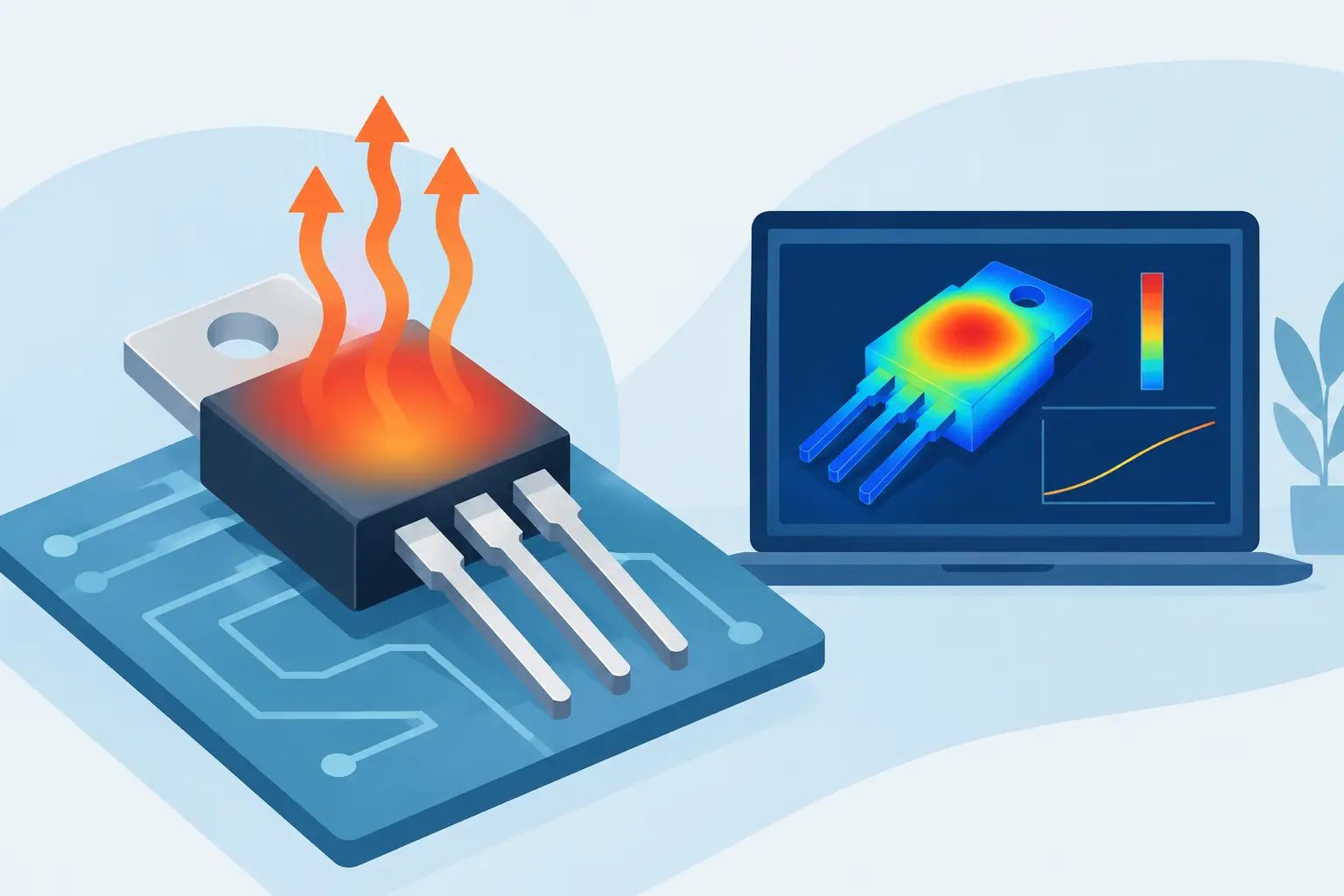
A transistor self heating guide starts with a practical observation: the electrical operating point and the thermal operating point are not independent. A device that appears acceptable under isothermal assumptions can shift threshold voltage, mobility, saturation current, leakage, and reliability margin once internally generated heat is allowed to alter the local lattice temperature. For power transistors, RF structures, densely packed logic, and devices with poor heat removal paths, that difference can determine whether a design is usable.
Self heating is therefore an electrothermal problem, not simply a post-processing temperature calculation. The current distribution establishes power dissipation. The resulting temperature field changes material properties and carrier transport. Those changes modify the current distribution and power again. A credible model must close that feedback loop with appropriate geometry, physical parameters, boundary conditions, and numerical controls.
What transistor self heating actually represents
In a semiconductor device, Joule heating is commonly represented by the local product of current density and electric field. Additional heat sources may arise from recombination, impact ionization, contact resistance, and energy relaxation mechanisms, depending on the transport model and device type. The heat equation then converts those sources into a spatial temperature distribution according to thermal conductivity, heat capacity for transient analysis, and heat flow through the surrounding structure.
The critical point is locality. A reported average device temperature can conceal a narrow hotspot near a drain-side gate edge, current-crowded contact, field plate termination, or constricted interconnect. That hotspot may control degradation even when the package-level temperature estimate appears moderate. Mesh resolution, source-term placement, and material interfaces consequently matter as much as the nominal total power.
For DC operation, the coupled solution seeks a steady state in which electrical power generation and heat removal balance. For pulsed operation, the thermal time constants of the active region, metallization, substrate, die attach, and package determine whether the device experiences a short-lived temperature spike or cumulative heating. A pulse width that is electrically brief may still be thermally significant if its repetition rate prevents adequate cooling.
Define the question before selecting the model
The necessary model complexity depends on the engineering decision. If the question is whether a modest bias shift changes channel temperature by a few degrees, a two-dimensional device cross-section with calibrated thermal boundaries may be sufficient. If the question concerns finger-to-finger temperature variation, via placement, substrate spreading, or a localized metallization bottleneck, a three-dimensional thermal model is generally required.
Start by defining the quantity to be trusted. It may be peak channel temperature, thermal resistance from hotspot to ambient, temperature-dependent drain current, a safe-operating-area limit, or the transient temperature response to a power pulse. This choice determines the geometry and physics that cannot be omitted.
A useful separation is between device-scale electrothermal coupling and structure-scale heat spreading. Device simulation resolves carrier transport, electric field, and heat generation in the active semiconductor. A larger thermal calculation resolves lateral spreading through the die, interconnect stack, package, heat sink, or neighboring heat sources. Combining every feature in one model is not automatically more accurate. It can introduce uncertain inputs and impractical mesh sizes. Use the model that resolves the mechanism controlling the result.
Build the electrical model before coupling temperature
An electrothermal calculation cannot correct an uncalibrated electrical model. Establish the isothermal device behavior first at relevant temperatures. Verify geometry, doping profiles, contacts, mobility, recombination, high-field transport, and any material-specific parameters against measured or otherwise credible reference data.
Temperature dependence must be physically consistent. Mobility commonly declines as lattice temperature rises, but the magnitude and functional form depend on scattering mechanisms and doping. Bandgap narrowing, intrinsic carrier concentration, saturation velocity, contact behavior, and thermal conductivity may also vary strongly with temperature. In wide-bandgap devices, high electric fields and substrate thermal properties can make these dependencies particularly consequential.
Do not treat thermal conductivity as a universal constant unless the anticipated temperature range justifies it. Silicon, silicon carbide, gallium nitride, metals, dielectrics, and interface layers can have very different temperature behavior. A constant value may be acceptable for an early comparison study, but it should be identified as an assumption rather than presented as a material prediction.
Represent heat sources where they occur
The simplest power estimate, terminal voltage multiplied by terminal current, is useful for a global energy check. It is not enough to locate a hotspot. The simulation should distribute heat generation according to the electrical solution, particularly in regions of high field or current crowding.
Check that the volume integral of modeled heat generation is consistent with net electrical power entering the device, subject to stored energy and boundary flux in transient cases. This energy-balance check catches sign errors, incomplete source terms, and contact definitions that can otherwise produce plausible-looking but incorrect temperature contours.
Thermal boundaries decide the result
A thermal model is only as defensible as its heat-removal path. Fixed-temperature boundaries are appropriate where a region is genuinely held near a known temperature, such as an idealized heat spreader reference plane. They are often overused at the backside of a thin substrate, where die attach, solder, carrier, and cooling hardware add substantial thermal resistance.
Convective boundaries require a realistic heat-transfer coefficient and ambient temperature. These values vary with airflow, surface orientation, enclosure geometry, and whether the device is attached to a heat sink. Radiation may be relevant at elevated temperatures or for exposed surfaces, but it rarely replaces a careful conduction model in packaged semiconductor assemblies.
Thermal boundary resistance at material interfaces deserves explicit attention. Perfect thermal contact between semiconductor, oxide, metal, solder, and ceramic layers can materially understate peak temperature. Conversely, assigning a large interface resistance without measurement or literature support can dominate the result for the wrong reason. Sensitivity analysis is the appropriate response when interface data are uncertain.
For early-stage work, state a range for uncertain boundary parameters and report the corresponding range of peak temperatures. A result such as 165 to 205 degrees C under credible interface assumptions is more useful than an unsupported prediction of 178 degrees C.
Mesh for gradients, not visual smoothness
Thermal gradients are usually sharp near localized heat sources, thin films, narrow contacts, and interfaces with large conductivity contrast. Refine the mesh in those areas and along the expected heat-flow path. A uniformly fine mesh can consume computation without improving the quantity of interest, while a coarse hotspot region can suppress the peak temperature and distort electrothermal feedback.
Perform a mesh-convergence study on at least the outputs that drive the decision: maximum lattice temperature, total dissipated power, drain current, and thermal resistance. Refine the mesh until further refinement produces an acceptably small change. The acceptable change depends on the task. A research study may require tighter control than an engineering screening calculation, but neither should rely on a single untested mesh.
For three-dimensional structures, mesh growth must be managed deliberately. SibLin is suited to thermal and related field calculations where spreading resistance, layered materials, and complex heat-flow paths require a numerical solution across large meshes. The value of a million-node capability is not the node count itself. It is the ability to place resolution at the hotspot and interfaces while retaining the full geometry needed to represent realistic heat removal.
Solve electrothermal feedback carefully
Fully coupled solutions can become difficult near strong nonlinearities. As temperature rises, reduced mobility may lower current under voltage bias and create negative feedback. In other conditions, leakage and temperature-dependent conduction can increase power and create positive feedback. The stability of the physical device and the stability of the numerical iteration are separate questions, although both must be examined.
A practical approach is to ramp bias or dissipated power gradually from a known low-power solution. Use temperature limits and residual checks to identify whether a calculation is converging toward a physical steady state or merely oscillating between inconsistent electrical and thermal states. Under current-controlled and voltage-controlled conditions, the same device may exhibit substantially different feedback behavior, so the external bias condition must match the intended application.
Transient simulation is necessary when the thermal time history affects performance or damage risk. Use time steps small enough to resolve fast electrical changes and early local heating, then allow larger steps as the response approaches slower package-scale thermal dynamics. Check time-step convergence just as carefully as spatial mesh convergence.
Report results that can be reviewed
A useful self-heating result includes more than a color temperature plot. Report the bias condition, ambient or reference temperature, electrical power, peak temperature and its location, boundary conditions, material thermal properties, interface assumptions, mesh-convergence evidence, and whether the solution is steady-state or transient. If possible, compare temperature-sensitive electrical characteristics with measurements, such as output-current roll-off, on-resistance shift, threshold shift, or pulsed versus DC behavior.
The most productive next step is usually not a larger model. It is an uncertainty-focused one: identify whether the prediction is limited by heat-source physics, interface resistance, boundary conditions, or insufficient spatial resolution, then improve that part of the model first.
Leave a Reply