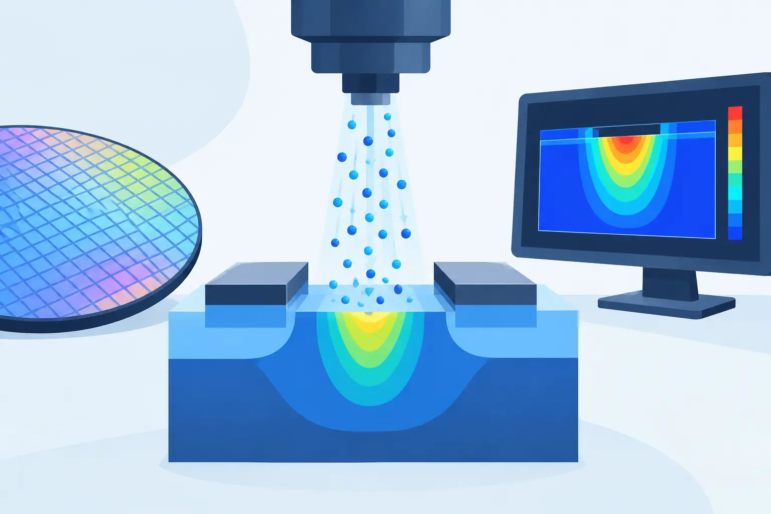
An implant profile that looks reasonable on a depth plot can still produce the wrong transistor. A small error in projected range, lateral straggle, activation, or anneal-driven diffusion can shift threshold voltage, junction leakage, sheet resistance, and breakdown behavior. That is why knowing how to model ion implantation means treating implantation as one calibrated stage in a connected process and device simulation flow, not as a single Gaussian profile.
For most semiconductor process work, the required level of detail depends on the decision being made. Early architecture studies may need fast, parameterized profiles. Process-transfer, device optimization, and failure analysis usually require a physics-based implant and anneal sequence tied to measured electrical and chemical data. The useful model is the simplest one that remains credible for the structure, species, energy range, and thermal budget under evaluation.
Define the physical question before selecting the implant model
Begin with the device quantity that the implant must predict. A source/drain implant may be evaluated through sheet resistance, junction depth, overlap capacitance, and short-channel behavior. A channel-adjust implant may be judged primarily by threshold voltage and its sensitivity to thermal processing. For a power device, the relevant concerns may be blocking voltage, field shaping, and implant-induced damage near a critical junction.
This choice determines what must be represented. A one-dimensional concentration-versus-depth profile can be sufficient for a blanket implant used in an initial diffusion calculation. It is not sufficient when mask edges, spacer geometry, tilt angle, lateral dopant penetration, or isolation structures influence the final device. In those cases, a two-dimensional process model is required because the lateral distribution is part of the electrical design.
Define the starting material as carefully as the implant itself. Crystal orientation, background doping, epitaxial layers, buried regions, oxide thickness, and existing topography affect the incident ion path and the subsequent thermal response. An incorrect initial structure cannot be repaired by adjusting dose after the fact.
Specify the implant conditions completely
An implant is characterized by more than species, dose, and energy. These inputs remain essential, but a credible process definition also includes tilt, twist or rotation, wafer orientation, screen layers, mask geometry, and whether the implant enters crystalline, amorphous, or partially damaged silicon.
Dose controls the total number of implanted ions per unit area. Energy controls the approximate depth distribution. Neither quantity alone determines the electrically active dopant profile. At low energy, a few nanometers of oxide, nitride, photoresist residue, or deposited film can change the silicon dose and projected range materially. At high dose, implant damage and amorphization may dominate the later activation behavior.
Tilt and rotation deserve explicit attention. They are often introduced to reduce channeling, but they also change lateral placement near mask edges and sidewalls. A vertical implant through a thin screen oxide can produce a very different profile from a tilted implant through a conformal layer. If the goal is to predict overlap under a gate or spacer, represent the actual geometry rather than applying a vertical one-dimensional profile beneath every exposed region.
Choose a profile model that matches the process window
Analytical implant models are efficient and useful when the process is well characterized and the device is not highly sensitive to detailed damage physics. Gaussian, dual-Pearson, or Pearson-type distributions can represent many implanted profiles using projected range, straggle, skewness, and kurtosis parameters. Their value is speed and transparency: an engineer can rapidly assess how a dose or energy split changes a junction.
Their limitation is that fitted moments do not necessarily describe channeling tails, complex mask-edge effects, or damage-dependent stopping. A profile may match the concentration peak while missing a low-concentration tail that controls a deep junction or punch-through path.
For structures where these effects matter, use a physically based implantation calculation or calibrated tabulated distributions. The selected method should account for ion stopping, scattering, crystal orientation where relevant, and lateral as well as vertical spread. Monte Carlo approaches can provide additional detail, particularly for low-energy implants and complex topography, but they require adequate particle statistics and computation time. They are not automatically the better choice if the uncertainty in anneal conditions or measurement data is larger than the added implant-model precision.
How to model ion implantation near masks and interfaces
The highest-value reason to use two-dimensional process simulation is usually geometry. Gate edges, spacers, STI corners, contact openings, and resist patterns create implant conditions that cannot be inferred from a blanket profile. Near these features, the simulation mesh must resolve material interfaces and the concentration gradients expected from lateral straggle.
Use finer mesh spacing at the silicon surface, beneath thin gate dielectrics, around implant-window edges, and at anticipated junction locations. Expand the computational region far enough from the active device that boundary conditions do not distort diffusion or electrical solutions. A coarse mesh can conserve total dose yet smear the peak concentration and move the extracted junction location.
Do not refine the entire structure indiscriminately. Fine elements should be concentrated where gradients, interfaces, and electrical fields demand them. This reduces runtime while preserving the detail needed for junction formation and later device simulation. Mesh convergence is a practical check: refine the relevant regions until key outputs such as junction depth, sheet resistance, and threshold voltage stop changing by a meaningful amount.
Model damage, activation, and annealing as a single sequence
The as-implanted dopant distribution is not the final electrical distribution. Ion implantation creates point defects and, at sufficiently high doses, amorphous regions. Subsequent annealing repairs damage, activates dopants, causes diffusion, and can introduce transient enhanced diffusion through excess interstitials. For boron, phosphorus, arsenic, and antimony, the balance among these effects differs substantially.
A useful anneal model must distinguish total chemical concentration from electrically active concentration. At high concentrations, clustering, solid solubility limits, and incomplete activation can prevent all implanted dopant atoms from contributing free carriers. Treating chemical concentration as active doping can substantially overestimate conductivity and distort device electrostatics.
Thermal processing should be entered as the actual sequence: pre-clean or oxidation steps when relevant, spike or soak anneals, ramp rates if the model supports them, and later thermal cycles that continue to move dopants. A short, high-temperature spike may yield a shallower activated junction than a longer furnace anneal at lower temperature. The outcome depends on species, damage state, concentration, and the complete thermal budget, not only on peak temperature.
Calibrate against measurements that constrain the model
Calibration should proceed from the quantities closest to the modeled physics. Use SIMS or comparable chemical profiling to constrain total dopant distribution. Use spreading resistance profiling, electrochemical capacitance-voltage data, Hall measurements, or sheet resistance to constrain active concentration and activation. Junction depth may be inferred from profiling or electrical test structures, provided the extraction definition is consistent between measurement and simulation.
Fit one physical uncertainty at a time. First verify dose retention and projected range for a blanket structure. Next fit the anneal response using activated profile or sheet-resistance data. Then introduce patterned geometry and compare lateral effects through suitable test structures. Trying to match a final transistor threshold voltage by changing several implant and diffusion parameters simultaneously can hide compensating errors.
Maintain separate parameter sets when process regimes are genuinely different. A low-dose channel implant, a high-dose amorphizing source/drain implant, and a through-oxide implant may not be represented credibly by one universal calibration. The objective is not a parameter set that matches every available curve imperfectly. It is a documented set of assumptions that predicts the intended process window reliably.
Carry the process result into device simulation
The final process mesh and active dopant distribution should feed the device calculation directly whenever possible. Poisson and carrier-transport solutions are sensitive to abrupt gradients, compensation, and the local location of junctions. Exporting the process result to a simplified analytical doping expression may remove precisely the lateral and activation effects that justified process simulation.
Check extracted electrical observables against the original modeling objective. For MOS structures, inspect threshold voltage, subthreshold slope, depletion extent, and gate-to-source/drain overlap. For diodes or power devices, evaluate junction capacitance, leakage, breakdown behavior, and peak electric field. If a result disagrees with measurement, identify whether the discrepancy is more likely due to geometry, implant placement, activation, transport assumptions, or contacts before changing model parameters.
A two-dimensional TCAD tool such as MicroTec is well suited to this workflow when the problem requires process geometry, diffusion profiles, and device behavior in one practical model. The aim is not to add every available physical option. It is to retain the effects that control the engineering decision and verify them against data.
A disciplined implantation model becomes most valuable when it can explain a measured trend, not merely reproduce one nominal profile. Build that traceability from implant recipe to anneal response to device metric, and the simulation remains useful when the next process split changes.
Leave a Reply