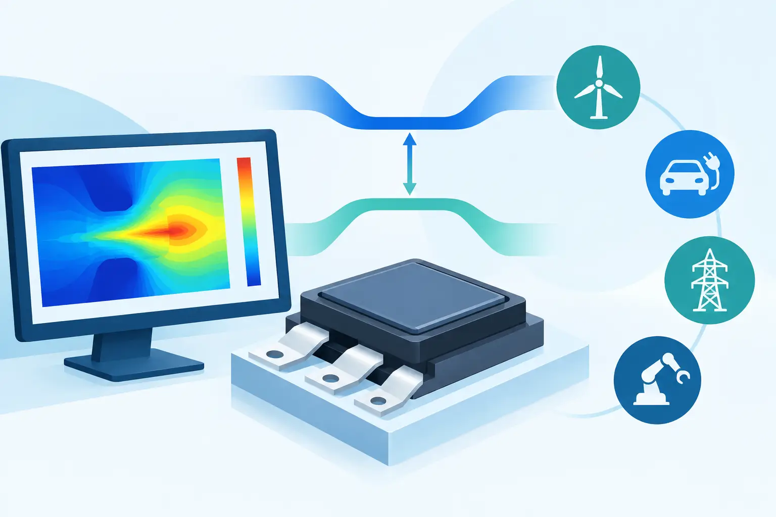
A silicon carbide MOSFET can meet its nominal blocking-voltage target in a simplified model and still fail the engineering review once oxide charge, edge termination, or localized heating are introduced. Wide bandgap simulation is valuable precisely because it exposes these dependencies before a wafer run converts them into schedule risk, yield loss, or an inconclusive failure analysis.
SiC and GaN are not simply silicon devices with larger bandgaps. Their attractive properties – high critical electric field, high-temperature capability, and low-loss switching potential – shift the dominant modeling questions. Field crowding can determine the practical voltage rating. Interface states can alter threshold behavior and channel mobility. Trapping can make the measured dynamic on-resistance depend on pulse history rather than a single DC operating point. A useful simulation workflow must represent the physical mechanism that limits the device, not just produce a plausible current-voltage curve.
What Wide Bandgap Simulation Must Resolve
The starting point is material definition. Bandgap, dielectric constant, carrier mobility, ionization coefficients, thermal conductivity, dopant activation, and recombination behavior should be treated as material- and temperature-dependent inputs where the operating condition requires it. Default silicon parameters are not an acceptable substitute, particularly for high-field or high-temperature studies.
For SiC power devices, incomplete dopant ionization may materially affect charge balance and resistance, especially across temperature. Avalanche and impact-ionization models require careful calibration because breakdown is strongly dependent on local electric field and device geometry. A result labeled as a breakdown voltage is only as useful as the mesh, ionization model, boundary conditions, and termination geometry behind it.
GaN introduces a different set of concerns. Polarization charge at heterointerfaces can establish the two-dimensional electron gas that defines HEMT operation. Surface conditions, buffer traps, and gate-stack effects may influence threshold voltage, current collapse, leakage, and transient behavior. The appropriate model detail depends on the question. An early layout comparison may need electrostatics and transport first; a reliability investigation may require trap kinetics, thermal coupling, and a pulse sequence that resembles the measurement method.
This is why a single “wide bandgap” setup is not meaningful. The device class, operating mode, and decision being supported determine the model set.
Start With the Engineering Decision
Simulation projects become inefficient when the team begins by enabling every available physical model. A more defensible approach begins with the decision that the result must support. Is the objective to compare implant conditions, set a drift-region dose, evaluate junction termination, estimate on-resistance, investigate gate leakage, or identify a thermal bottleneck? Each objective suggests a different domain, mesh strategy, and calibration plan.
Process simulation is appropriate when fabrication history determines the device structure. Implantation, diffusion, oxidation, activation, and etching establish profiles that cannot always be represented accurately by idealized analytic junctions. In SiC, the distinction between implanted and electrically active dopant profiles may be central to predicting channel or junction behavior. A two-dimensional process and device workflow can preserve that connection from process conditions to electrical response.
Device simulation is appropriate when the geometry and doping are established and the question concerns electrostatics, carrier transport, capacitance, breakdown, or transient response. Solving Poisson, continuity, and relevant transport equations provides the physical basis for evaluating field distribution and current flow. However, the calculated result should not be mistaken for validation. Calibration against measured profiles, test structures, published material data, or known device characteristics remains necessary.
Thermal simulation becomes essential when power density and switching behavior make temperature nonuniform. Electrical characteristics in SiC and GaN are temperature dependent, while local heat generation depends on electrical current density and resistance. This feedback can change the location and severity of the limiting condition. A uniform ambient-temperature assumption may be acceptable for an initial device comparison, but it is often inadequate for high-power operation or packaging decisions.
Mesh Control Is a Physical Requirement
Wide bandgap devices often contain the sharp gradients that expose weak meshing practices: depletion boundaries, gate edges, heterointerfaces, field plates, trench corners, and junction termination extensions. A coarse mesh can underestimate a peak electric field while still showing an apparently smooth potential distribution. That is not a minor numerical discrepancy when the design margin depends on avalanche onset or dielectric stress.
Mesh refinement should follow the expected physics. Refine around corners, interfaces, depletion fronts, and regions of high current density. Then perform a mesh-convergence study on the quantity that drives the decision, such as peak field, breakdown voltage, gate leakage, or on-resistance. A result is not converged because the solver reached a numerical tolerance. It is converged when further physically targeted refinement no longer changes the engineering conclusion beyond an acceptable margin.
Boundary conditions deserve the same scrutiny. Contact models, thermal anchors, surface charge assumptions, and symmetry planes can materially affect the answer. For a lateral GaN device, the source, drain, gate, passivation, and substrate or buffer assumptions form part of the model, not peripheral details. For a vertical SiC device, backside contact conditions and termination extent can determine whether the simulated field pattern corresponds to a realizable structure.
Model Transients and History When Measurements Do
DC curves remain useful, but they do not answer every wide-bandgap question. Dynamic RDS(on) in GaN, for example, can depend on prior high-voltage stress, off-state duration, temperature, and measurement delay. A DC model that omits trapping may match one transfer curve while missing the operating behavior that matters in a converter.
The practical response is not to build the most elaborate trap model immediately. First reproduce the relevant stress-and-measurement sequence. Define initial conditions, bias intervals, temperature, and observation time. Then add only the trap distributions and capture or emission parameters needed to test a credible mechanism. If several parameter sets fit one measurement, use additional observables such as temperature dependence, recovery time, or spatially resolved potential to distinguish them.
This discipline also applies to switching studies. Parasitic inductance, external circuit conditions, and thermal time constants may matter as much as intrinsic device equations. The appropriate simulation boundary can extend from a two-dimensional active device region to a coupled electrothermal problem, depending on whether the task is device optimization or system-level prediction.
Match Dimensionality to the Failure Mechanism
Two-dimensional TCAD is often the efficient choice for cross-sectional structures, process development, vertical power devices, and lateral devices whose dominant variation lies in one plane. It provides direct access to doping profiles, potential contours, carrier concentrations, current density, and high-field regions without imposing the computational cost of a full three-dimensional model.
Three-dimensional analysis becomes necessary when the controlling mechanism is inherently three-dimensional. Examples include nonuniform die heating, package conduction paths, current spreading under contacts, irregular heat sources, and geometries where edge effects cannot be represented by a cross section. The decision should be based on the physics, not a preference for a larger model.
For engineering groups that need both levels of analysis, a practical division of work is often effective: use two-dimensional process and device simulation to narrow the design space, then apply three-dimensional thermal, Poisson, diffusion, drift-current, or spreading-resistance calculations to the structures where geometry and heat flow demand it. Siborg’s MicroTec and SibLin reflect this separation of workloads rather than forcing every problem into a single software bundle.
Calibration Is the Difference Between a Plot and a Prediction
A simulated output becomes useful when it is compared against evidence. Begin with quantities that can be measured with reasonable confidence: sheet resistance, threshold voltage, capacitance-voltage response, forward current-voltage behavior, breakdown distribution, or thermal resistance. Calibrate the simplest model that accounts for these observables, then test whether it remains credible across bias and temperature conditions.
There are trade-offs. A detailed model may improve agreement for one device generation but introduce parameters that are difficult to identify independently. An idealized model may be better for comparing geometric alternatives if all candidates share the same assumptions. The key is to state the purpose and uncertainty clearly. Simulation is most valuable when it ranks options, identifies sensitivities, and shows where measurement effort will reduce risk.
For wide bandgap devices, the productive question is rarely whether simulation can reproduce every measured point. It is whether the model identifies the field, interface, thermal path, or transient mechanism that will govern the next design decision. Build the model around that question, verify the numerical controls, and let the result direct the next experiment or layout change.
Leave a Reply