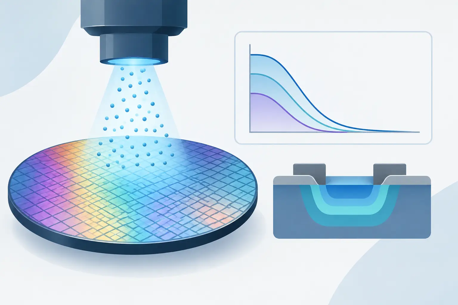
A junction depth value does not define a device. Neither does sheet resistance, by itself. The electrical behavior of a diode, transistor, resistor, or detector depends on the complete dopant distribution: its lateral extent, vertical gradient, peak concentration, compensation, and relation to surrounding regions. Diffusion profile modeling for semiconductor devices turns process assumptions into that distribution before a wafer run makes those assumptions expensive.
The engineering value is not a color contour plot. It is the ability to determine whether a proposed thermal cycle produces the intended junction location, whether lateral diffusion consumes a critical spacing budget, and whether the resulting concentration profile supports the required electric field and carrier transport. A useful model must therefore preserve the connection between process history, physical mechanisms, geometry, and device response.
The diffusion profile is a device input
Dopant diffusion is often introduced through Fick’s laws, but practical semiconductor processing quickly moves beyond a constant diffusivity model. Diffusivity can vary strongly with temperature, dopant concentration, crystal orientation, point defects, oxidation conditions, and transient enhanced diffusion. At high concentrations, the distinction between chemical concentration and electrically active concentration also becomes material to the final result.
For process engineers, the question is usually not whether diffusion occurs. It is which mechanism controls the profile under a particular sequence of implant, drive-in, oxidation, anneal, deposition, and etch steps. A short high-temperature step may preserve a steep gradient while moving the junction less than a longer furnace cycle. The longer cycle may improve activation or uniformity, but its lateral spread can reduce isolation margin or alter a transistor’s effective channel geometry.
That is why a one-dimensional analytical profile is often adequate for early estimates but insufficient for layout-sensitive structures. Once a diffused region approaches an oxide edge, a mask opening, a buried layer, or another doped region, two-dimensional process simulation becomes the more credible representation. The vertical and lateral components are coupled by the actual geometry.
Start with credible process inputs
A diffusion calculation can be numerically stable and still be wrong because its initial conditions are wrong. The starting dopant distribution should represent the preceding process as closely as the available data allows. For implanted species, this commonly includes projected range, straggle, dose, and any channeling assumption. For predeposition, it may involve a surface concentration or finite source condition.
Thermal history deserves equal care. Temperature is not merely an entry in a recipe table. Diffusion is highly temperature dependent, so an error in ramp duration, peak temperature, or hold time can produce a materially different profile. If the furnace cycle includes oxidation, the model should account for whether segregation and moving boundaries affect the dopant distribution. Boron near silicon dioxide, for example, cannot always be treated with the same assumptions used for an inert anneal.
Calibration should use measurements that constrain the intended result. SIMS can provide concentration-versus-depth information, though interpretation near interfaces and at low concentrations requires care. Spreading-resistance profiling can characterize electrically active dopants over useful ranges. Sheet resistance, junction staining, and electrical test structures add complementary constraints, but none should be treated as a universal substitute for profile data.
A practical calibration sequence begins with a simple structure whose process history is well documented. Match the measured vertical profile or junction depth first, then test whether the same parameter set predicts a lateral feature. Parameters should not be adjusted independently for every structure unless the physical conditions genuinely differ. Otherwise, calibration becomes curve fitting rather than a process model.
Choose model complexity by the decision at stake
The simplest model that resolves the engineering question is generally the right choice. For a long drive-in from a known source, a one-dimensional approximation may establish a useful temperature or time window. For a shallow junction under a narrow opening, it may conceal the principal failure mechanism: lateral encroachment.
Diffusion profile modeling in semiconductor devices should expand in complexity when geometry or coupled physics changes the decision. Two-dimensional simulation is appropriate when mask edges, field oxides, wells, contacts, or adjacent diffusions influence the concentration contours. It is also appropriate when the device simulation requires a physically consistent structure rather than independently specified Gaussian profiles.
More physics is not automatically better. Adding concentration-dependent diffusion, point-defect effects, clustering, segregation, and moving interfaces introduces parameters that must be supported by process knowledge or measurement. If those parameters are uncertain, an elaborate model can create false confidence. The useful standard is predictive value: does the added mechanism improve agreement with measured behavior across more than one condition?
Numerical control matters near junctions and interfaces
Diffusion profiles can contain steep gradients over distances much smaller than the full device dimension. A mesh that is too coarse smooths those gradients, shifts a calculated junction, and weakens the predicted electric field. A uniformly fine mesh, however, can increase runtime and memory requirements without improving results in regions where the solution varies slowly.
Mesh refinement should follow physics and geometry. It belongs around implant peaks, shallow junctions, material interfaces, mask edges, contact windows, and regions that later govern depletion width or current flow. The model should be checked for mesh convergence by refining critical areas and comparing quantities that affect the design decision, such as junction depth, sheet resistance, peak field, or breakdown voltage.
Time stepping requires similar discipline. Large thermal time steps can miss rapid early redistribution, particularly where diffusivity changes sharply with temperature or concentration. Very small steps everywhere can make routine process exploration inefficient. Adaptive control is useful when it maintains accuracy during fast transients without imposing the same computational cost on quiet portions of the thermal cycle.
Mass conservation is another essential check. Unless the modeled process includes a physical source, loss mechanism, or segregation pathway, the total dopant inventory should remain consistent. Unexpected gain or loss can reveal a boundary-condition error, insufficient domain extent, or a numerical setting that needs review.
Carry the profile into electrical simulation
The purpose of a process profile is usually an electrical decision. A physically generated concentration distribution can be transferred to device analysis to solve Poisson and drift-current equations under bias. This step exposes effects that a junction-depth target alone cannot show.
A profile with the correct metallurgical junction may still create an unfavorable electric-field peak. A resistor diffusion may meet sheet-resistance requirements while producing excessive voltage dependence because of its surrounding isolation. In a bipolar structure, a base profile affects not only base width but also gain, transit time, and punch-through margin. For MOS-related processes, well and channel distributions influence threshold voltage, depletion behavior, and short-channel effects.
This linkage is also where compensation must be handled correctly. Net doping determines much of the electrostatic behavior, but separate donor and acceptor distributions may be necessary when activation, recombination, or process interpretation requires them. Treating all profiles as a single net concentration can obscure the mechanism behind a measured electrical result.
For a two-dimensional process-to-device workflow, Siborg’s MicroTec is designed to model semiconductor fabrication steps and evaluate the resulting device structure without requiring a larger software suite. The appropriate simulator should match the dimensionality and equations of the problem. A process engineer establishing diffusion contours has a different workload from a researcher solving coupled three-dimensional diffusion, thermal, or electrostatic behavior over a mesh exceeding one million nodes.
Use simulation to narrow experiments, not replace them
A calibrated diffusion model is most valuable when it reduces the number of wafers needed to answer a focused question. It can compare thermal budgets, test mask-bias sensitivity, estimate junction movement after a revised anneal, or identify which process variable deserves experimental control. It cannot compensate for an undocumented furnace cycle, uncertain implant dose, or incomplete material data.
Maintain traceability between each simulation and its assumptions. Record the diffusion model, parameter source, thermal cycle, boundary conditions, geometry, mesh settings, and comparison data. When a later measurement disagrees with prediction, this record makes it possible to isolate whether the issue lies in the process record, model selection, numerical resolution, or measurement interpretation.
The most useful diffusion profile is not the most detailed image. It is the one that gives an engineering team a defensible reason to change a process condition, protect a layout margin, or proceed to fabrication with fewer unknowns.
Leave a Reply