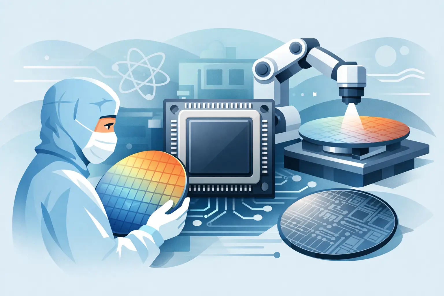
A transistor layout is only an intention until semiconductor processing turns it into controlled material structure on a silicon wafer. For engineers asking what is semiconductor processing, the useful answer is not simply “chip manufacturing.” It is the ordered set of physical and chemical operations used to create active devices and interconnects with dimensions, dopant concentrations, film properties, and alignment tolerances that must remain within specification across an entire wafer.
The process links device physics to manufacturing reality. A device designer may specify a threshold voltage, junction depth, contact resistance, or gate dielectric thickness. Process integration must determine which thermal cycles, deposition methods, lithographic masks, etches, implants, and cleaning steps can produce those results repeatedly.
What Is Semiconductor Processing?
Semiconductor processing is the fabrication of electronic devices by selectively modifying semiconductor wafers. Silicon is the most common starting material, although silicon carbide, gallium nitride, gallium arsenide, indium phosphide, and other materials are used where their electrical, optical, thermal, or high-voltage characteristics justify the added process complexity.
A typical wafer moves through hundreds or thousands of individual operations. These are not independent steps. Each one changes the conditions for the next. An oxidation may consume silicon and alter dimensions. An ion implant establishes a dopant distribution, but a later anneal changes its depth and electrical activation. An etch creates the intended feature geometry, yet can also introduce sidewall damage or leave residues that affect a subsequent deposition.
The result is a layered structure containing transistors, diodes, resistors, capacitors, isolation regions, contacts, and metal interconnects. In integrated-circuit production, these structures are repeated many times across a wafer and later separated into individual dies. In discrete power devices, sensors, and optoelectronic components, the sequence and geometry differ, but the same principle applies: controlled material modification creates useful electronic behavior.
The Core Operations in Semiconductor Processing
The exact flow depends on the device, material system, feature size, and fabrication facility. Still, most process flows are built from a common set of operations.
Wafer preparation and thermal processing
Manufacturing begins with a polished wafer that must meet demanding requirements for crystal quality, flatness, particle contamination, and surface condition. Initial cleaning removes organic residues, metals, particles, and native oxides that could create defects or cause poor film adhesion.
Thermal processing then changes the wafer through high-temperature exposure. Thermal oxidation, for example, grows silicon dioxide that can serve as an insulating layer, a masking layer, or part of a gate structure. Diffusion drives dopant atoms into the wafer through elevated-temperature exposure. Annealing repairs crystal damage after implantation and electrically activates dopants.
Temperature history is central to process control. Dopant movement is cumulative, so every high-temperature step can alter a previously established profile. A process engineer is therefore concerned not only with peak temperature but also with ramp rates, dwell time, ambient chemistry, and the full thermal budget.
Thin-film deposition
Devices require films that are conductive, insulating, semiconducting, or protective. Common deposition approaches include physical vapor deposition, chemical vapor deposition, atomic layer deposition, electroplating, and epitaxial growth.
Film selection is governed by more than nominal thickness. Engineers assess uniformity across the wafer, step coverage over topography, density, stress, stoichiometry, impurities, electrical resistivity, dielectric constant, and interface quality. A film that is acceptable on a flat monitor wafer may fail in an actual device if it does not cover narrow trenches or high-aspect-ratio features adequately.
Epitaxy is a special case in which a crystalline layer is grown with a defined relationship to the substrate. It is particularly important for structures requiring controlled doping and low defect density, including some power devices, bipolar devices, and compound-semiconductor components.
Photolithography and pattern transfer
Photolithography defines where subsequent processing will occur. The wafer is coated with photoresist, exposed through a mask or reticle, and developed to leave a patterned resist image. That pattern becomes a temporary stencil for etching, implantation, deposition, or lift-off.
Critical lithographic concerns include linewidth, overlay accuracy, focus, exposure dose, resist profile, and defect density. Overlay error is especially consequential in multilayer devices because features on one layer must align correctly with features already present below it. As dimensions shrink, small variations in pattern placement can change transistor length, parasitic capacitance, or contact overlap.
Lithography does not create the final device structure by itself. It transfers geometric information into a process mask. The following etch, implant, or deposition determines how that information becomes physical material geometry.
Etching and material removal
Etching selectively removes material from exposed regions. Wet etches use liquid chemistries and may be isotropic or crystallographically selective. Dry etches use plasma-based processes and can provide the anisotropy needed for vertical sidewalls and fine patterns.
Selectivity, etch rate, profile control, uniformity, and endpoint detection all matter. An etch must remove the target film without damaging the underlying layer or excessively consuming the mask. Plasma conditions may also affect electrical performance through charging damage, residue formation, or altered surface chemistry.
The trade-off is often direct. A highly anisotropic process can preserve critical dimensions but may have lower selectivity or introduce more sidewall effects. A gentler wet process may provide excellent selectivity but lack the directional control required for advanced interconnect or transistor features.
Doping and junction formation
Doping establishes n-type and p-type regions by adding controlled concentrations of donor or acceptor atoms. Ion implantation is widely used because it provides dose control and can be spatially patterned using photoresist or hard masks. Diffusion remains useful in certain processes and is fundamental to understanding how dopant profiles evolve during thermal treatment.
The key output is not merely dopant dose. Device behavior depends on the final electrically active concentration as a function of depth and lateral position. Implant energy, dose, tilt, channeling, pre-amorphization, anneal conditions, and nearby material boundaries can all affect the result.
For a MOS device, changes in channel doping and junction profiles can shift threshold voltage, leakage, breakdown behavior, and series resistance. For a power device, vertical doping profiles often determine the trade-off between on-resistance and blocking voltage. These are problems where process simulation is valuable because electrical performance cannot be inferred from mask geometry alone.
Metallization, planarization, and passivation
Once device regions are formed, contacts and interconnects connect them into circuits. This stage can involve barrier layers, metal deposition, patterning, dielectric deposition, via formation, and copper electroplating. Modern multilevel interconnect requires careful control of resistance, capacitance, electromigration risk, and contact integrity.
Chemical-mechanical planarization removes topography so later lithographic levels remain within focus requirements. It is a necessary capability for complex multilayer structures, but it introduces its own sources of variation, including dishing, erosion, and within-wafer nonuniformity.
A final passivation layer protects the device from moisture, contamination, and mechanical damage. Pad openings are then created for wire bonding, flip-chip attachment, probing, or other packaging methods.
Why Process Integration Is a Physics Problem
Process integration is the discipline of making individual modules work as a coherent device flow. A successful deposition recipe is not enough if its film stress causes pattern distortion. A correct implant may still produce the wrong junction after downstream oxidation and annealing. A low-resistance contact can become unreliable if the cleaning sequence leaves interfacial contamination.
This is why semiconductor processing relies on coupled physical models. Diffusion and oxidation affect geometry and concentration profiles. Poisson and drift-current equations connect those profiles to electrical behavior. Heat transfer becomes important in anneals, high-power devices, packages, and reliability studies. Mechanical stress and thermal expansion can also influence film integrity and device characteristics.
Simulation is most useful when it answers a bounded engineering question: whether a proposed thermal cycle produces the required two-dimensional dopant profile, how a process change affects a junction, or whether a three-dimensional structure can dissipate heat within a specified temperature limit. Siborg Systems develops standalone tools for these distinct workloads, including two-dimensional process and device simulation and three-dimensional numerical analysis of heat transfer, Poisson, diffusion, and drift-current problems.
From Process Flow to Measured Device Performance
No process model replaces measurement. Fabrication teams use test structures, monitor wafers, metrology, electrical characterization, defect inspection, and reliability testing to determine whether the physical wafer matches its intended design. Thickness measurements, sheet resistance, critical-dimension data, implant monitoring, capacitance-voltage curves, and current-voltage measurements each expose different parts of the process.
The practical objective is correlation. A model should be checked against measured profiles and device data, then used to reduce the number of experimental iterations required for the next design or process revision. The appropriate model detail depends on the decision being made. Early development may require fast estimates of diffusion behavior; failure analysis may justify a detailed two-dimensional or three-dimensional solution.
Semiconductor processing is therefore best understood as controlled cause and effect. Every material change has a physical consequence, and every electrical specification imposes constraints on the process sequence. Engineers who preserve that connection between fabrication conditions, material structure, and measured device behavior make better use of both wafer experiments and simulation.
Leave a Reply