Blog

  • How to Simulate Wafer Annealing in TCAD

    How to Simulate Wafer Annealing in TCAD

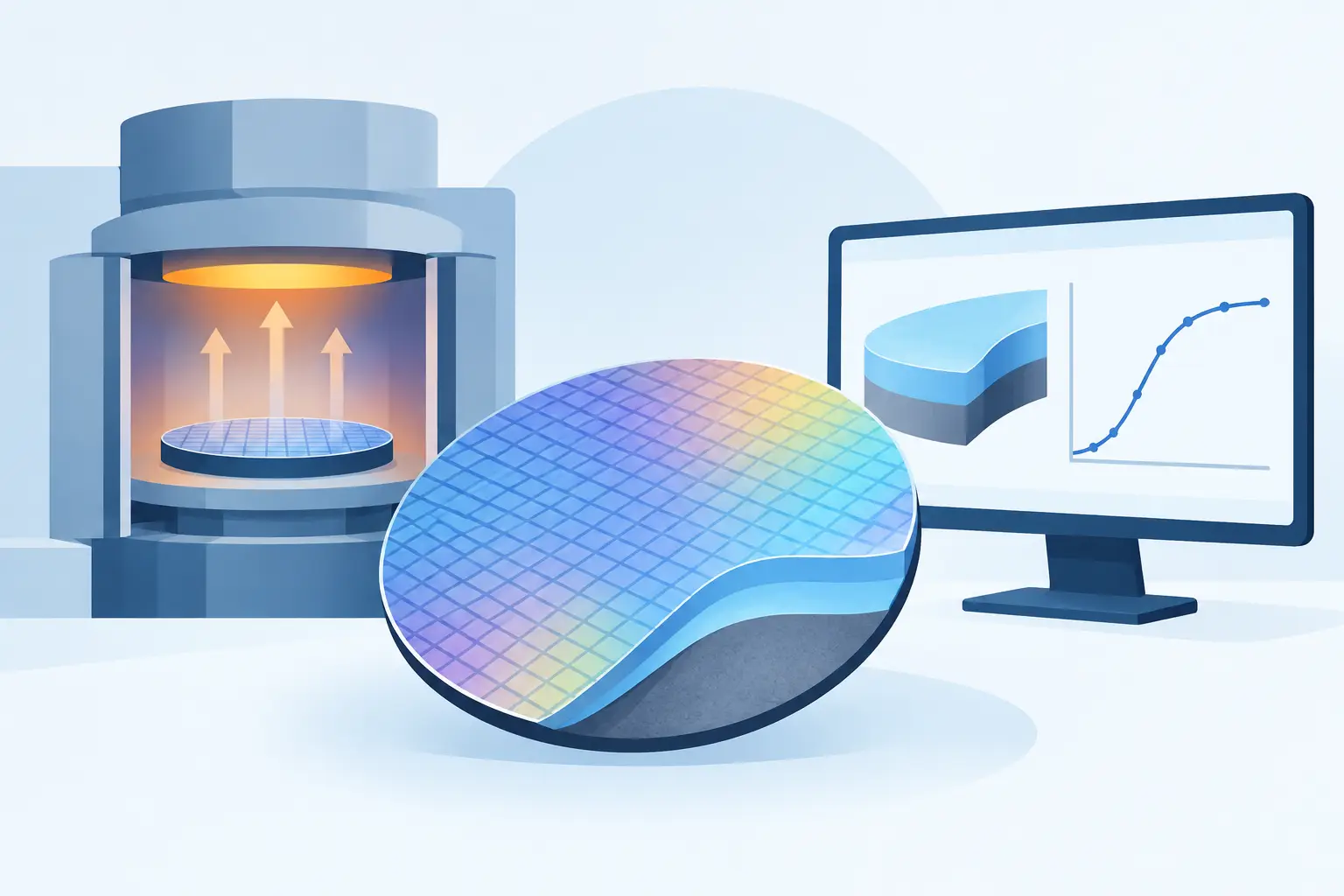
    An anneal step can determine whether an implanted junction meets its sheet-resistance target, preserves a shallow profile, or diffuses far enough to compromise short-channel control. That is why learning how to simulate wafer annealing starts with the process objective, not with selecting a temperature from a furnace recipe. The simulation must represent the thermal history and the mechanisms that redistribute and electrically activate dopants during that history.

    For most process studies, wafer annealing is not an isolated calculation. It follows implantation, deposition, oxidation, or a preceding diffusion step, and its result becomes the starting profile for later etches, implants, or device simulation. A credible model therefore carries the wafer structure and impurity distributions forward through the full relevant sequence.

    Define the anneal result before building the model

    Start by specifying the quantity that will be used to judge the run. A junction depth extracted at a stated concentration, sheet resistance, active dopant dose, peak concentration, or lateral encroachment can each be valid targets. They do not necessarily respond to the same model assumptions in the same way.

    For example, a drive-in anneal after a deep implant may be evaluated primarily by vertical junction depth. A rapid thermal anneal for a source-drain extension is more sensitive to transient diffusion, activation, and the steepness of the near-surface profile. If the anneal is part of a bipolar or power-device flow, the relevant question may instead be whether a long thermal budget moves dopant across a buried interface or alters a collector profile.

    This distinction matters because a model calibrated only to junction depth can still produce an incorrect sheet resistance. Electrical activity depends on more than total chemical concentration. It can be affected by clustering, precipitation, compensation, and the local defect population.

    Build the correct pre-anneal wafer state

    The anneal calculation is only as useful as its initial condition. Construct the substrate, epitaxial layers, deposited films, oxide regions, and implanted regions that exist immediately before heat treatment. Preserve material boundaries because they can change diffusion behavior and serve as sources or sinks for point defects.

    For implanted wafers, use an implantation model that establishes a physically reasonable as-implanted profile, including lateral distribution when geometry makes it relevant. Dose and energy alone are not sufficient if the application depends on channeling tails, screen oxide effects, tilt, rotation, or masking topology. A one-dimensional approximation may be acceptable for a blanket implant far from pattern edges; it is usually not sufficient for a patterned shallow junction.

    The inputs that should be documented for every anneal run include:

    • wafer orientation, substrate type, background dopant, and starting concentration
    • implant species, dose, energy, tilt, rotation, and any screen or sacrificial oxide
    • layer materials and thicknesses present during the thermal step
    • furnace or rapid-thermal temperature history, including ramps and holds
    • ambient conditions, especially when oxidation or nitridation occurs during annealing

    The objective is traceability. When a measured profile and a simulated profile disagree, an engineer should be able to separate uncertainty in the implant condition from uncertainty in the diffusion or activation model.

    Represent the thermal budget, not just peak temperature

    A nominal anneal temperature is an incomplete process description. Diffusion depends strongly on temperature, so time spent in the ramp can be material for short, high-temperature recipes. Two cycles with the same peak temperature and dwell time can produce different profiles when their ramp rates differ substantially.

    Define the complete temperature-time sequence: ramp-up, stabilization if applicable, main soak, ramp-down, and any separate preheat or post-anneal cycle. For conventional furnace diffusion, the soak commonly dominates the thermal budget. For spike and rapid thermal anneals, ramp segments may account for a meaningful fraction of dopant motion and defect evolution.

    Use measured or equipment-qualified temperature profiles when they are available. A recipe setpoint is not always the wafer temperature, particularly during fast transients or with differing wafer emissivity and chamber loading. If the purpose of the study is process-window prediction, run credible upper and lower thermal-budget cases rather than treating one nominal profile as exact.

    Ambient must also be explicit. An oxidizing ambient can inject interstitials and grow oxide, changing the near-surface diffusion behavior of some dopants. An inert anneal may preserve a different defect balance. Treating these cases as identical can give a numerically clean result that does not describe the actual wafer process.

    Select diffusion and activation physics to match the regime

    The simplest diffusion treatment uses concentration-dependent diffusivity. It may be suitable for long, moderate-dose drive-in steps where empirical calibration data supports the approximation. It is not automatically adequate for high-dose implants or modern thermal cycles.

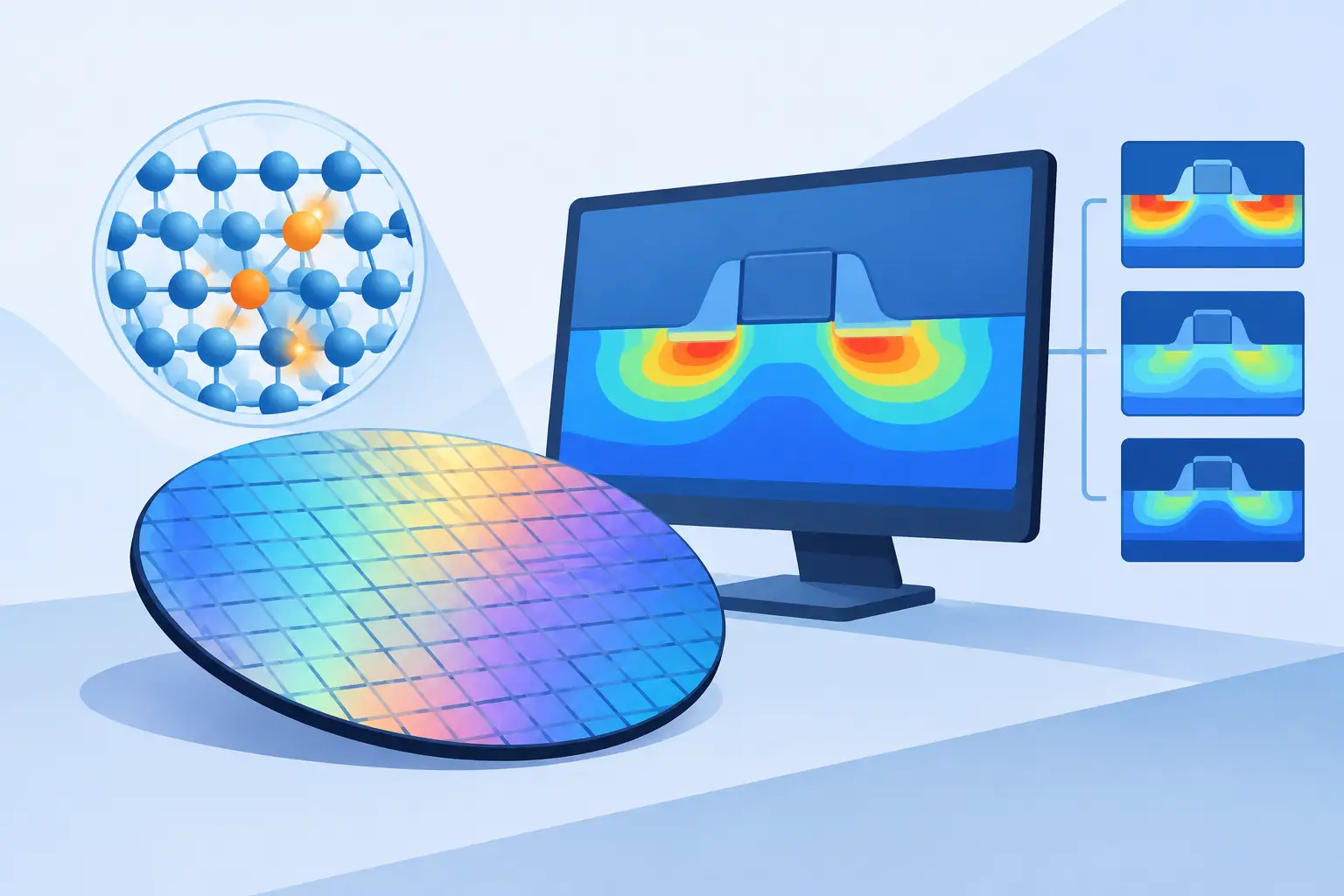
    Ion implantation creates excess vacancies and interstitials. During subsequent annealing, their evolution can cause transient enhanced diffusion, particularly for dopants whose transport couples strongly to point defects. At high concentrations, clustering and incomplete activation can limit the electrically active fraction even when the chemical dose is unchanged. Interfaces, oxidation, and damage-removal kinetics further affect the result.

    Choose the least complex physics set that addresses the measured behavior and intended decision. Adding mechanisms without calibration can create more adjustable parameters than useful predictive power. Conversely, omitting transient diffusion or activation in a shallow-junction study can force an engineer to compensate with unrealistic diffusivity values.

    A practical calibration sequence is to first match the as-implanted profile, then match a limited set of annealed chemical profiles, and finally compare electrical observables such as sheet resistance or spreading-resistance data. Keep the calibration set independent from the experiments used to evaluate prediction. Otherwise, agreement may only show that the model has been fitted to the same data.

    Use mesh refinement where gradients and interfaces demand it

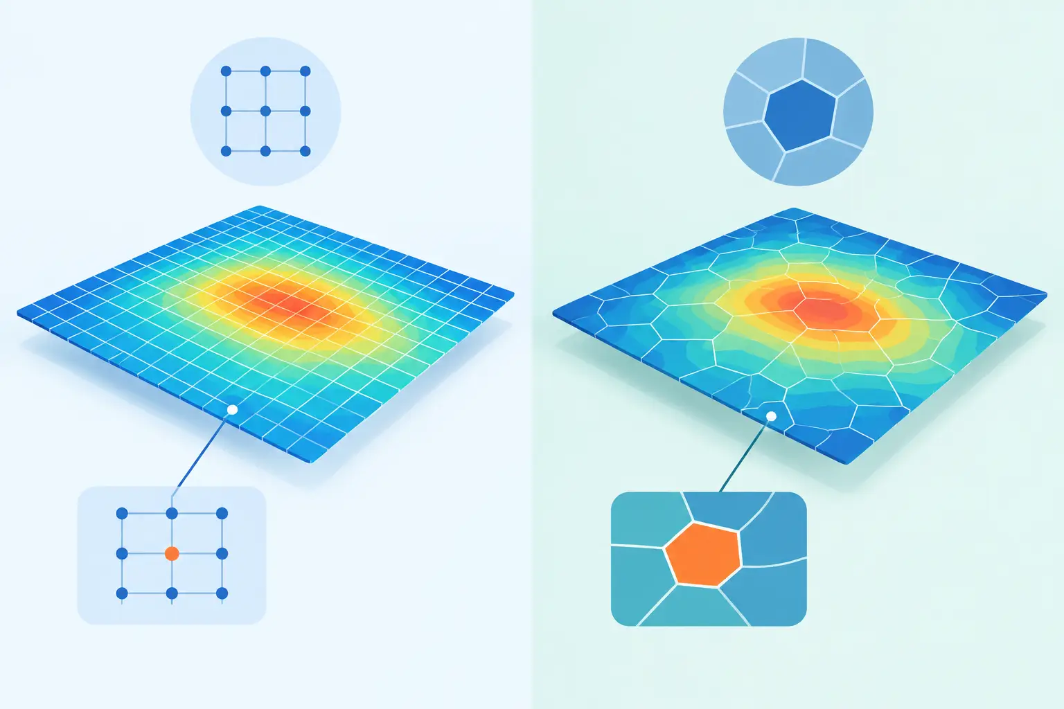
    Annealing simulations solve coupled transport behavior across concentration gradients that can be steep near the surface, at junctions, and around mask or spacer edges. Mesh resolution should be concentrated in those regions rather than distributed uniformly across a large substrate depth.

    In two-dimensional process simulation, refine the mesh around implant windows, oxide-silicon interfaces, shallow junctions, and locations where lateral diffusion affects device dimensions. Extend the domain deeply enough that the lower boundary does not influence the region of interest. A boundary placed too near a diffusing profile can artificially retain or remove dopant, depending on its condition.

    Perform a mesh-convergence check before trusting extracted values. Reduce local cell size and compare junction depth, peak active concentration, sheet resistance, and lateral spread. If these outputs shift materially with refinement, the original grid was not adequate. The best mesh is not the finest possible mesh; it is the coarsest mesh that produces stable engineering outputs within the required tolerance.

    Validate outputs against measurements that answer different questions

    Plotting concentration versus depth is necessary, but it is not sufficient. Compare the simulated chemical and active profiles separately when data permits. Secondary-ion mass spectrometry measures chemical concentration, while sheet resistance, electrochemical capacitance-voltage methods, or spreading-resistance measurements provide different evidence about activation and electrically relevant profiles.

    When comparing junction depth, state the concentration criterion and whether it refers to total or active dopant. When comparing sheet resistance, ensure that carrier mobility and compensation assumptions are consistent with the extracted quantity. A close match to one measurement can conceal an error in another.

    Sensitivity analysis is especially useful near a process limit. Vary dose, peak temperature, dwell time, ramp rate, and selected model parameters within credible uncertainty bands. If a small temperature change produces a large junction-depth shift, the process is thermally sensitive and simulation should report a range, not only a nominal value.

    Choose the dimensionality that matches the question

    A vertical blanket diffusion can often be studied efficiently in one dimension during early calibration. Once mask edges, spacers, isolation regions, or neighboring implants affect the outcome, use a two-dimensional process model. The extra dimension is justified when lateral diffusion changes an electrically important length or overlap.

    MicroTec v4.23 is suited to this two-dimensional process and device workflow, allowing engineers to carry process-defined dopant profiles into later electrical analysis without purchasing an unnecessary software bundle. For thermal problems that require full three-dimensional heat-transfer analysis, the thermal field should be established with a tool designed for that dimensionality before simplifying it into an appropriate process thermal history.

    Treat anneal simulation as a controlled engineering model

    The useful deliverable is not a color contour of dopant concentration. It is a documented model that states the starting structure, thermal cycle, physical assumptions, mesh criteria, calibration evidence, and extracted metrics. That record allows another engineer to reproduce the result, challenge an assumption, or apply the model to a nearby process condition.

    Wafer annealing is sensitive to details that are easy to omit: a few seconds of ramp time, an oxidizing ambient, a damaged implant tail, or a boundary placed too close to the active region. Account for the details that control the decision, calibrate against more than one observable, and let the required process tolerance determine how much model complexity is justified.

  • TCAD Meshing Guide for Accurate Device Models

    TCAD Meshing Guide for Accurate Device Models

    A mesh can make a physically correct TCAD model appear wrong. An abrupt junction represented by too few elements may shift a predicted breakdown voltage; a coarse oxide interface can suppress the field peak that drives tunneling or reliability concerns. This TCAD meshing guide treats mesh design as part of the model definition, not as a final numerical setting applied after the structure and equations are chosen.

    The practical objective is not to create the finest possible grid. It is to place resolution where material properties, dopant concentration, potential, carrier density, temperature, or current density change on a short length scale. Everywhere else, unnecessary nodes consume memory and increase solve time without improving the engineering result.

    TCAD Meshing Guide: Start With the Physics

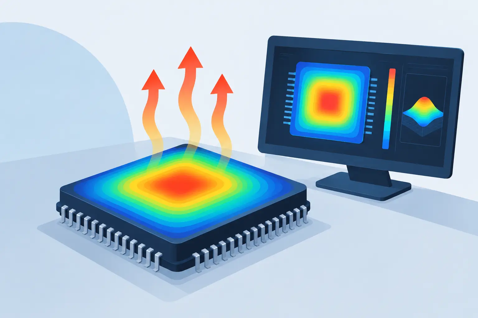
    Before setting mesh lines or activating refinement, identify the quantity that will determine the design decision. A process simulation may require accurate dopant contours after implantation, diffusion, oxidation, and annealing. A device simulation may instead depend on threshold voltage, channel current, junction leakage, peak electric field, or breakdown behavior. Thermal and spreading-resistance problems require resolution around heat sources, material boundaries, narrow current paths, and temperature gradients.

    This distinction matters because a process mesh and a device mesh do not necessarily have the same requirements. During diffusion, the mesh must resolve steep concentration gradients near implanted layers and junctions. During electrical solution, the critical regions may move to the gate dielectric, channel, depletion boundary, drain-side high-field region, or contact edges. Remeshing between process and device stages is often more efficient than carrying a uniformly dense process grid into the electrical calculation.

    Characteristic physical lengths provide a useful starting point. These can include junction depth, oxide thickness, channel length, depletion width, diffusion length, thermal penetration depth, and the radius of curvature at a contact or field plate. The smallest relevant feature is not always the smallest geometric feature. A thin passive layer may need limited resolution if it has little effect on the result, while a slightly wider depletion region may require close attention because it controls the electric field distribution.

    Put Nodes Where Gradients and Interfaces Occur

    A good initial mesh is deliberately nonuniform. Fine spacing belongs at semiconductor-oxide interfaces, heterojunctions, p-n junctions, narrow conductive paths, contact boundaries, corners, and regions with expected field crowding. Coarser spacing is appropriate in electrically quiet bulk regions, provided the transition into refined zones is gradual.

    At a material interface, nodes should align with the interface rather than allowing elements to cut across it. Material parameters can change abruptly across silicon, oxide, metal, or compound semiconductor boundaries. If the interface is poorly represented, the discrete equations may blur a discontinuity that is central to the problem. This is particularly consequential for normal electric field, displacement continuity, thermal flux, and carrier transport near boundaries.

    Junctions require comparable care. A doping profile can be smooth in a mathematical sense while still changing over a distance too short for a coarse mesh to capture. Resolve the region on both sides of the metallurgical junction, not simply the point where donor and acceptor concentrations cross. For reverse-biased devices, extend adequate refinement through the depletion region and toward the location of peak field. For forward conduction, check the regions where current crowding and quasi-Fermi potential gradients develop.

    Corners deserve special treatment, but not unlimited refinement. Sharp geometric corners can create very high local fields in an idealized two-dimensional model. If the fabricated device has a rounded corner, represent that radius where practical. If the geometry must remain sharp, use local refinement and interpret singular or near-singular peaks cautiously. A single maximum field value at one corner is less useful than a mesh-converged field distribution over the physically meaningful region.

    Control Element Quality, Not Only Spacing

    Small elements alone do not guarantee a reliable solution. Excessive aspect ratios, abrupt changes in neighboring element size, and poorly shaped triangles or quadrilaterals can degrade conditioning of the discretized equations. The symptoms are familiar: slow convergence, sensitivity to solver tolerances, oscillatory potential or carrier profiles, and results that move when a seemingly unrelated region is refined.

    Use smooth mesh grading between fine and coarse regions. The permissible growth rate depends on the solver, equation set, and geometry, but a gradual transition is generally preferable to a single jump from nanometer-scale spacing to a much larger bulk element. In regions dominated by one-dimensional variation, elongated elements may be reasonable. Near curved interfaces, contacts, and multidirectional current flow, more balanced elements are usually safer.

    For thermal analysis, mesh quality should follow heat-flow paths rather than geometry alone. A fine grid directly beneath a localized heat source may be necessary, but the surrounding material must also be sufficiently resolved to carry the spreading heat flux. For a three-dimensional problem, refining only through the thickness while leaving lateral spacing coarse can underestimate lateral spreading resistance or distort the peak temperature location.

    Build the Mesh in Controlled Passes

    A disciplined workflow prevents mesh density from becoming an uncontrolled response to every convergence issue. Begin with a baseline mesh that resolves all interfaces and the expected active device regions. Solve the simplest relevant physical case first, such as equilibrium, a low-bias operating point, or steady-state heat flow. This establishes whether geometry, boundary conditions, and material assignments are correct before nonlinear effects are introduced.

    Next, refine one region at a time according to the quantity of interest. If threshold voltage is the target, refine the gate dielectric, channel, and source/drain junction regions before adding nodes elsewhere. If avalanche or breakdown is being studied, focus on the high-field junction curvature, depletion region, and dielectric boundaries. If thermal resistance is the result of interest, refine the heat source, interfaces with thermal conductivity contrast, and the volume through which heat spreads to the sink.

    After each refinement, compare engineering outputs rather than only visual plots. Useful checks include terminal current, threshold voltage, peak field location, integrated charge, total power, maximum temperature, and extracted resistance. A mesh is approaching adequacy when these values change by less than the tolerance justified by the design decision. The tolerance should be tighter for model verification or publication-quality parameter extraction than for an early feasibility study.

    A practical mesh-convergence record should identify the node count, minimum local spacing, refined regions, solver settings, and the resulting key metrics. This record makes later results defensible and helps distinguish physical changes from numerical ones. It also prevents a common mistake: comparing two simulations that differ in both physical assumptions and mesh resolution, then attributing the difference to only one cause.

    Use Adaptivity With Engineering Judgment

    Adaptive meshing can be valuable when gradients are not known in advance. Error estimators or solution-based criteria can add resolution where potential, carrier concentration, temperature, or dopant gradients become steep. This is particularly useful for complex junction geometries and three-dimensional heat-flow problems with localized sources.

    Adaptivity is not a substitute for physical judgment. It may refine a numerical feature caused by an unsuitable boundary condition, an unrealistic sharp corner, or insufficient model calibration. Review where nodes are added and ask whether the region corresponds to a real mechanism. If a mesh repeatedly concentrates at a boundary far from the active device, the boundary placement or condition may need revision rather than more elements.

    For large three-dimensional calculations, set a node budget before refinement begins. A million-node mesh can be appropriate for a detailed thermal, Poisson, diffusion, drift-current, or spreading-resistance problem, but only when the additional resolution changes the decision-relevant result. The right simulator is the one that matches the equation set and dimensionality of the problem, not a larger software bundle than the analysis requires.

    Validate Against More Than Convergence

    Mesh convergence establishes that the numerical discretization is no longer dominating the result. It does not prove that the physical model is correct. Compare simulated junction depths, sheet resistance, capacitance, I-V curves, thermal resistance, or field profiles with measurement, established analytical limits, or trusted reference structures whenever available.

    Also check conservation. Terminal currents should balance within the expected numerical tolerance. Applied power should correspond to generated and removed heat in a steady-state thermal calculation. Potential and flux behavior at symmetry planes, insulating boundaries, and contacts should agree with the stated boundary conditions. These checks often reveal setup errors earlier than a denser mesh will.

    The useful mesh is the smallest one that reproduces the physical quantity needed for the decision, with stable results under local refinement. Treat it as an engineering artifact worth documenting. That discipline produces simulations that are faster to run, easier to review, and more credible when their results guide a device or process choice.

  • How to Choose TCAD Software for Students

    How to Choose TCAD Software for Students

    A semiconductor device course becomes more useful when students can test the consequences of a process step rather than only calculate them on paper. With the right TCAD software for students, a class can move from a diffusion profile or doping concentration to junction behavior, electric fields, carrier transport, and device characteristics using the same physical relationships encountered in engineering practice.

    The key is not to give every student the largest available simulation suite. A better choice is software that matches the course problem, exposes the governing physics clearly, and runs reliably within the hardware and time limits of an academic lab. For introductory device physics, a focused two-dimensional process and device simulator can be more instructive than an enterprise platform whose setup, licensing, and model selection become the main lesson.

    Start With the Physics the Course Must Teach

    The first selection question is simple: what must students be able to model by the end of the course? TCAD covers a broad range of semiconductor simulation tasks, and the appropriate tool depends on whether the work centers on fabrication, device operation, electrothermal effects, or three-dimensional structures.

    For a semiconductor technology course, students may need to model oxidation, diffusion, implantation, annealing, and the resulting dopant distributions. A device-physics course may begin with a previously defined structure and concentrate on Poisson and carrier-transport equations, depletion regions, current-voltage curves, breakdown, or capacitance. A thermal-analysis assignment may require heat transfer, diffusion, and electrical current spreading in a three-dimensional package or substrate.

    These are related problems, but they do not require the same solver or workflow. Asking students to use a three-dimensional mesh for a planar MOS structure can add computational cost without improving the lesson. Conversely, forcing a fundamentally three-dimensional heat-spreading problem into a two-dimensional model can hide the behavior students need to understand.

    Two-dimensional simulation is often the right teaching scale

    Many foundational semiconductor structures are naturally introduced in cross section. A two-dimensional simulator lets students see how process history produces a device geometry, then observe how that geometry affects potential, carrier concentrations, electric fields, and terminal behavior. The visual connection between fabrication and electrical response is especially valuable when students are still learning to interpret band diagrams and equations.

    Two-dimensional models also support shorter iteration cycles. Students can change a diffusion time, oxide thickness, junction depth, or bias condition and obtain a result during a lab period. That speed matters. A simulation assignment should reward thoughtful parameter changes and comparison with theory, not encourage students to submit one long job and wait for results they cannot investigate.

    Evaluate TCAD Software for Students by Workflow

    Academic software should not eliminate technical rigor, but it should avoid making routine setup unnecessarily difficult. Students need to spend their attention on mesh placement, boundary conditions, material parameters, and physical models. They should not lose most of a laboratory session resolving installation conflicts or navigating a workflow designed around large corporate design teams.

    A practical student workflow usually has four stages: define or import a structure, select the relevant process or device models, specify contacts and boundary conditions, then examine numerical and physical results. Each stage should be explicit enough that an instructor can relate it to course material.

    For example, if an assignment investigates a pn junction, students should be able to identify the doping profile, inspect the mesh near the junction, apply a bias sweep, and determine whether the computed depletion width and current trends agree with analytical expectations. If results differ, the software should provide enough visibility for students to distinguish a physical effect from an inadequate mesh or incorrect boundary condition.

    This is where focused software has an advantage. A broad suite can be justified for a research group that models many device classes and process flows. For a class with defined learning objectives, a disciplined interface and a direct simulation path are often more valuable than a long catalog of modules students will never use.

    Numerical reliability is part of the curriculum

    Students should learn that a converged result is not automatically a credible one. TCAD assignments are a useful way to teach mesh sensitivity, solver limits, model validity, and the importance of comparing simulation with measurements or analytical estimates.

    That requires numerical algorithms that behave predictably. If a solver fails without meaningful diagnostic information, students may assume semiconductor equations are arbitrary or inaccessible. If it converges too easily under inappropriate assumptions, they may not recognize the limits of the model. Good instructional software supports controlled experiments: refine the mesh, change the bias step, alter a physical parameter, and observe whether the conclusion remains stable.

    Faculty should also consider whether the solver is appropriate for the intended equation set. Poisson, diffusion, drift-current, and heat-transfer problems impose different numerical demands. A program selected because it is familiar or inexpensive may still be a poor fit if it cannot represent the governing physics of the assignment.

    Licensing and Deployment Affect Whether Students Can Practice

    A technically capable simulator is of limited value if students can only access it from one departmental workstation. Modern courses often combine scheduled lab time with independent work, so deployment should be considered alongside physical models and solver performance.

    Standalone licensing can be particularly practical for a course or research group with a specific simulation requirement. It avoids requiring students to learn and administrators to maintain a large bundled environment when only one process, device, or field-solver capability is needed. It can also make budget planning clearer for departments that need to equip a lab without committing to software modules outside their curriculum.

    The right licensing model depends on enrollment and course structure. A small graduate seminar may work well with a limited number of lab licenses and supervised projects. A larger undergraduate course may need broader access, especially if assignments involve iterative work outside scheduled sessions. Before selecting a package, instructors should establish how many concurrent users are expected, whether remote access is needed, and how students will exchange input files and results.

    Documentation matters as much as access. Students need examples that begin with a known physical problem and explain why a particular model, contact definition, or mesh region was chosen. Faculty need enough technical detail to create assignments that are demanding without becoming fragile. The most useful documentation supports both audiences: it gives beginners a reproducible starting point while providing advanced users the specifications required to extend the model.

    Match the Tool to the Level of the Student

    Undergraduate and graduate users do not necessarily need different software, but they do need different expectations. In an undergraduate course, the instructor may provide a baseline structure and ask students to vary process conditions or bias. The goal is to establish physical intuition and confirm concepts introduced in lecture.

    Graduate students and research assistants should take greater responsibility for model selection, mesh design, parameter calibration, and result validation. They may use TCAD to investigate a thesis question, reproduce a published structure, or establish a preliminary design before fabrication. At this level, the ability to inspect intermediate results and control numerical assumptions becomes essential.

    A package that supports both groups can be useful when the same department teaches device physics and conducts semiconductor research. Siborg’s MicroTec v4.23, for example, is a two-dimensional process and device simulator used in more than 130 universities across 27 countries. That type of established academic deployment matters because it indicates that the software has been applied in instructional settings as well as technical simulation work.

    Still, adoption figures should not replace evaluation. Instructors should test a representative assignment before committing to a course workflow. Use a problem with known behavior, such as a one-dimensional-like pn junction represented in two dimensions, then assess installation, runtime, convergence, output clarity, and the effort required for students to reproduce the result.

    Build Assignments Around Interpretation, Not Button Presses

    The strongest TCAD exercises ask students to make and defend engineering judgments. A useful assignment does more than request a plot of current versus voltage. It asks why a curve changes when junction depth, oxide thickness, carrier lifetime, or temperature changes, and whether the change is physically plausible.

    Students should be required to record model assumptions and numerical settings. They should explain mesh placement near high-gradient regions, identify boundary conditions, and compare at least one simulation outcome with an analytical approximation or published measurement. This practice prepares them for industrial and research environments, where a result must be reviewed, not merely generated.

    There is also value in assignments that show what the model cannot answer. A two-dimensional simulation may provide strong insight into a planar device while remaining insufficient for a package-level thermal path. A drift-diffusion model may be appropriate for one device regime and inadequate for another. Teaching these boundaries gives students a more durable skill than familiarity with any single interface.

    The best choice is the simulator that lets students spend their limited time asking better questions about semiconductor physics. When the software matches the dimensionality, equations, and scale of the problem, simulation becomes what it should be in an academic setting: a disciplined way to connect theory, process decisions, and observable device behavior.

  • Semiconductor Simulation Software for Universities

    Semiconductor Simulation Software for Universities

    A graduate device-physics course can move quickly from a one-dimensional junction derivation to a question that cannot be answered on a whiteboard: how do implant conditions, diffusion, geometry, contacts, and temperature change the electrical behavior of an actual structure? Semiconductor simulation software for universities gives students and researchers a practical way to test those relationships before committing time and budget to fabrication or measurement.

    The useful choice is not necessarily the largest TCAD suite. A university needs software that matches the physics being taught or investigated, operates reliably on available computing resources, and remains accessible to students who are learning semiconductor engineering rather than administration of a complex software platform.

    What universities need from semiconductor simulation software

    University requirements differ from those of a high-volume commercial fab. Teaching laboratories need repeatable examples, understandable inputs, and results that students can relate directly to equations from coursework. Research groups need sufficient physical rigor to investigate process conditions, device structures, thermal behavior, or current spreading without reducing the problem to an oversimplified approximation.

    Those needs often coexist. An instructor may use the same tool to demonstrate dopant diffusion in an undergraduate course, supervise a master’s project on a MOS structure, and support doctoral research involving coupled electrical and thermal effects. The software should therefore have a learning curve appropriate for occasional users while retaining numerical methods suitable for serious analysis.

    Licensing also matters. Departmental procurement is rarely simple, and research groups often work with finite grant periods. Standalone licensing for a clearly defined simulator can be more practical than adopting an enterprise bundle whose unused modules increase both cost and training demands.

    Start with the engineering problem, not the software category

    The phrase TCAD covers a wide range of workloads. Selecting software by label alone can leave a university with capabilities it does not use and gaps in the work it actually performs. The first decision is dimensionality and governing physics.

    Two-dimensional process and device studies

    Two-dimensional simulation is appropriate for many foundational semiconductor questions. It can model process sequences that establish doping profiles, then calculate device behavior based on the resulting structure. This workflow is particularly useful when students must connect fabrication steps to electrical characteristics rather than treating process and device physics as separate topics.

    A two-dimensional technology computer-aided design tool should support the core sequence: define geometry and materials, model diffusion or implantation effects, establish contacts and boundary conditions, solve the relevant device equations, and examine quantities such as potential, carrier concentration, electric field, and current. For instruction, the value lies in seeing how a changed process parameter propagates into a changed device response.

    Two-dimensional analysis is also often the right research choice when a cross section captures the dominant physics. It requires fewer computational resources than a full three-dimensional model and makes parameter studies more manageable. The trade-off is clear: it cannot represent effects dominated by out-of-plane geometry, localized heat flow, or genuinely three-dimensional current paths.

    Three-dimensional thermal and field problems

    When the problem is inherently spatial, a three-dimensional numerical solver becomes necessary. Heat spreading through a package or substrate, current crowding near contacts, nonuniform potential in a complex structure, and diffusion in a large volume cannot always be represented credibly in two dimensions.

    For these cases, evaluators should look at the equations the solver can treat and the mesh sizes it can handle. A solver for heat transfer, Poisson, diffusion, drift-current, and spreading-resistance problems gives a university lab a focused numerical foundation for electrical and thermal studies. Mesh capacity matters because practical device and package geometries can quickly require hundreds of thousands of nodes. For advanced work, the ability to solve meshes exceeding 1,000,000 nodes may be the difference between analyzing the intended structure and simplifying it beyond usefulness.

    Three-dimensional simulation has costs. Mesh preparation, memory demand, solution time, and interpretation are more demanding. It should be chosen because the physics requires it, not because a three-dimensional model appears more sophisticated.

    The teaching test: can students relate outputs to physics?

    A simulator is most effective in a university setting when it reinforces physical reasoning. Students should be able to change an input, state what they expect to happen, run the calculation, and explain any difference between expectation and result. Software that produces attractive plots without exposing the assumptions behind them has limited instructional value.

    In semiconductor courses, useful assignments commonly ask students to compare junction profiles after changes in diffusion time or temperature, study the impact of doping on depletion behavior, or examine how geometry affects field concentration. The best exercises do not ask students merely to operate menus. They require interpretation of boundary conditions, material parameters, mesh resolution, and convergence behavior.

    That last point is important. Numerical simulation should not be presented as a replacement for analytic device physics. It is a way to extend it. A student who understands why Poisson’s equation, carrier transport, and continuity relationships matter is better prepared to judge whether a calculated result is physically credible.

    Faculty should also consider how easily simulation cases can be reused. A well-designed set of baseline projects can serve multiple course sections and be expanded for advanced students. Consistency is especially valuable when teaching assistants support labs or when students work across different computers.

    The research test: are the algorithms and assumptions defensible?

    Research use requires more than a convenient interface. Graduate students need confidence that the solver formulation, boundary treatment, mesh strategy, and convergence controls are suitable for the problem. A simulation result can guide an experiment, motivate a device redesign, or appear in a thesis. In each case, the numerical basis must withstand scrutiny.

    This does not mean every research group needs a broad, all-purpose platform. It means the selected product must be specific about what it solves. A process and device simulator should clearly support the semiconductor modeling tasks assigned to it. A three-dimensional field solver should explicitly address the thermal, electrostatic, diffusion, and current-flow equations relevant to the study.

    Verification remains the responsibility of the researcher. Results should be checked against limiting analytical cases, published measurements, known material behavior, or independent calculations where possible. Mesh refinement is particularly important: if a result changes materially when the mesh is improved near a junction, interface, or contact, the earlier solution was not yet sufficiently resolved.

    Evaluate workflow and support before procurement

    A short technical evaluation should use a representative university problem, not a generic demonstration example. For a device group, that may be a diffusion profile followed by a diode or transistor calculation. For a thermal group, it may be heat flow through a multilayer structure with realistic boundary conditions. The goal is to determine whether users can reach interpretable results with a reasonable setup effort.

    During evaluation, ask whether the input model can be documented for a thesis or lab report, whether output data can be examined beyond a single image, and whether the software runs predictably on the department’s available hardware. Also establish who will maintain example files and provide first-line help to students. Even specialized software benefits from a local faculty member, researcher, or lab coordinator who understands the intended workflow.

    Long-term product history is relevant. University courses and research programs outlast individual student cohorts, so continuity matters. Siborg Systems has developed specialized semiconductor and numerical simulation software since 1994, and its MicroTec simulator has been deployed at more than 130 universities in 27 countries. That kind of institutional use is meaningful when a department needs software that can support recurring instruction as well as focused research projects.

    A practical selection standard

    The appropriate semiconductor simulation software for universities is the tool that lets a department solve its real problems with credible physics and manageable effort. For process and device courses, a focused two-dimensional simulator may provide the strongest balance of learning value and computational efficiency. For advanced heat-transfer, field, and spreading-resistance research, a three-dimensional solver with large-mesh capability may be the necessary complement.

    The procurement question is therefore direct: pick the simulator that matches the problem, not a bundle you do not need. Students gain clearer insight when the model is understandable, and researchers gain more useful results when the numerical method fits the geometry and physics under investigation.

  • Large Scale Finite Difference Meshes in 3D

    Large Scale Finite Difference Meshes in 3D

    A million-node model is not merely a smaller simulation with more grid points. A large scale finite difference mesh changes the numerical problem: memory use becomes material, mesh spacing affects matrix conditioning, and boundary assumptions can dominate the result. For three-dimensional semiconductor, thermal, and electrical-field analysis, the mesh must represent the physical geometry without making the solution impractical to obtain or difficult to verify.

    Finite difference methods remain a direct and effective approach when the geometry can be represented on structured or logically structured grids. They are particularly useful for Poisson, diffusion, heat-transfer, drift-current, and spreading-resistance problems where engineers need clear control of node placement, material properties, source terms, and boundary conditions. The practical question is not whether more nodes are available. It is whether those nodes resolve the physics that drives the engineering decision.

    What a Large Scale Finite Difference Mesh Changes

    At small scale, it is often possible to refine the entire domain and accept the additional computational cost. That approach stops being economical in a three-dimensional device, package, wafer region, or heat-spreading structure. Doubling the resolution in each spatial direction increases the number of unknowns by roughly eight times. Depending on the solver and stored coefficients, memory demand and solution time can rise even more sharply.

    A mesh with 1,000,000 or more nodes also produces a different linear-algebra workload. The discretized equations form a sparse system, but sparse does not mean inexpensive. Storage format, ordering, preconditioning, convergence tolerance, and the contrast between neighboring material properties all affect the time required to reach a useful solution.

    This matters especially when conductivity, permittivity, or thermal diffusivity changes abruptly across interfaces. A coarse representation of a thin insulating layer, contact region, or high-conductivity path may produce a solution that appears numerically converged while failing to represent the local gradient correctly. Solver convergence alone is not evidence that the mesh is physically adequate.

    Start With the Physical Length Scales

    Mesh density should follow the shortest length scale that materially affects the requested output. In thermal analysis, that may be a narrow heat source, a thin interface layer, or the region near a temperature-sensitive component. In an electrical problem, it may be a contact edge, depletion region, junction transition, current-crowding location, or a constricted spreading-resistance path.

    The requested result determines where refinement belongs. If the objective is junction temperature, nodes should be concentrated around heat generation and thermal bottlenecks rather than distributed uniformly through distant substrate volume. If the objective is terminal resistance, refinement is most valuable where current lines converge, material properties change, or the potential gradient is steep.

    Uniform grids are easy to construct and inspect, but they can waste most of the available node count in regions where the field is nearly linear. Nonuniform spacing can reduce the total number of nodes substantially, provided that changes in cell size are gradual enough to avoid unnecessary discretization error and poor conditioning. The correct choice depends on the geometry, governing equation, and whether local peak values or integrated quantities are the primary deliverable.

    Thin Regions Require Deliberate Treatment

    Thin layers are a recurring source of misleading results. If a layer is represented by only one or two grid intervals, its effective thermal or electrical resistance may depend more on mesh placement than on the specified material parameter. Adding nodes across the layer is often necessary, but not always sufficient. The interface condition and the interpretation of material properties at adjacent nodes must also be consistent with the discretization scheme.

    When a thin region is below the practical resolution of the full model, an equivalent boundary or interface condition can be preferable. This reduces node count while preserving the relevant resistance or transfer behavior. It is a modeling decision that should be documented, tested, and revisited if the design changes.

    Boundary Conditions Are Part of the Model

    Large domains can create false confidence. A model may include extensive surrounding material and still use a boundary condition that distorts the solution. Fixed-temperature, adiabatic, fixed-potential, symmetry, flux, and mixed boundary conditions each make a specific physical claim. They should be selected from the actual test condition or operating environment, not from convenience.

    For thermal simulations, the distance between a heat source and an artificial fixed-temperature boundary can strongly affect predicted peak temperature. For Poisson or spreading-resistance simulations, an imposed potential boundary placed too close to the region of interest can alter field lines and current paths. Extending the domain is one remedy, but it increases the number of unknowns. A better boundary model may be equally important.

    Symmetry deserves similar scrutiny. It can reduce a three-dimensional computation dramatically when geometry, material properties, excitation, and boundary conditions are genuinely symmetric. If a heat source is offset, a contact is asymmetric, or material placement differs across the assumed plane, symmetry can suppress the very effect under investigation.

    Accuracy Must Be Demonstrated, Not Assumed

    Mesh-convergence testing is the central verification step for a large scale finite difference mesh. The purpose is not to identify the largest mesh a workstation can hold. It is to show that the engineering quantity of interest changes acceptably as the mesh is refined.

    A useful study begins with a baseline mesh and repeats the calculation with refinement concentrated in critical regions. Compare the outputs that will support the design decision: maximum temperature, voltage drop, total current, extracted resistance, field maximum, or location of a hotspot. Global quantities can converge before local gradients do, so both should be examined when local reliability or breakdown risk matters.

    A practical record should state the node count, minimum and maximum spacing, boundary placement, solver tolerance, and the measured change between mesh levels. This makes the result reviewable by another engineer and prevents later comparisons from mixing changes in physics, geometry, and numerical resolution.

    Analytical limits and simplified benchmark cases are also valuable. A uniform slab, one-dimensional diffusion case, or known resistance geometry can expose sign errors, incorrect boundary implementation, and unit inconsistencies before a full three-dimensional model is used. Such tests are faster than diagnosing an unexpected result in a million-node production calculation.

    Solver Strategy and Memory Discipline

    The governing equation determines the matrix characteristics, while the mesh determines its size and conditioning. Direct methods can be appropriate for modest systems or special matrix structures, but their memory requirements can become prohibitive as three-dimensional node counts rise. Iterative methods are commonly more practical for large sparse systems, particularly when paired with a preconditioner appropriate to the equation and coefficient distribution.

    Tolerance selection requires judgment. An unnecessarily tight residual target can consume substantial run time without changing the reported temperature or resistance. A loose target can leave a visible error in a local peak or produce unstable results when comparing design variants. Residual behavior should be interpreted alongside changes in the physical output, not treated as an isolated pass-fail number.

    Memory planning should include more than the node count. Arrays for material properties, source terms, boundary flags, solution vectors, matrix coefficients, and solver workspace all contribute. The difference between a calculation that fits comfortably in memory and one that relies heavily on disk paging can determine whether parameter studies are feasible.

    For workloads involving three-dimensional heat transfer, Poisson, diffusion, drift-current, or spreading resistance, SibLin v1.2 is designed for numerical solutions on meshes exceeding 1,000,000 nodes. The relevant capability is not the node count alone, but the ability to define the appropriate equation, material distribution, and boundary conditions for the physical problem being evaluated.

    Build the Mesh Around the Decision

    The most useful mesh is not necessarily the finest one. It is the one that gives stable, defensible answers for the measurement or design choice at hand within available computational resources. A package-level temperature estimate may justify coarser treatment of remote volumes. A study of contact crowding or a localized hot spot may require significant refinement in a comparatively small region.

    Before committing to a large run, establish the output of interest, identify the regions that control it, and perform a focused convergence check. Then retain enough information to reproduce the model when geometry, material data, or operating conditions change. That discipline turns a large numerical calculation into an engineering result that can be reviewed, compared, and acted upon.

  • Electrical Field Solver Software for Real Devices

    Electrical Field Solver Software for Real Devices

    A field solution that looks plausible on screen can still be inadequate for design work. A coarse mesh can obscure field crowding at a contact edge. An inappropriate boundary condition can produce an apparently stable potential distribution that has no physical meaning. Electrical field solver software must therefore do more than display contours: it must solve the governing equations on a geometry, mesh, and boundary model that represent the device being evaluated.

    For semiconductor engineers, device physicists, and thermal-analysis researchers, the selection question is direct. Does the solver match the dimensionality, physics, mesh scale, and intended engineering decision? The right answer is often a focused numerical tool, not the largest available software bundle.

    What electrical field solver software should solve

    At its core, an electrical field calculation begins with potential. For electrostatic and many steady-state conduction problems, Poisson’s equation relates potential to charge density and material permittivity. The electric field follows from the spatial gradient of that potential. In a uniform, charge-free region, the problem may reduce to Laplace’s equation. These equations are foundational, but their implementation determines whether a calculation remains useful when geometry and materials become realistic.

    In semiconductor structures, charge is rarely an independent input. Carrier concentrations, ionized dopants, applied bias, and transport can be coupled to the potential solution. A field solver used for device analysis may therefore need to work alongside diffusion and drift-current equations rather than treat the electric field as an isolated electrostatic result. The appropriate model depends on the question. Estimating depletion-region behavior in a two-dimensional junction is different from resolving current spreading through a three-dimensional contact structure.

    Material interfaces matter as much as equations. Dielectric discontinuities alter normal electric displacement. Ohmic contacts, insulating boundaries, symmetry planes, fixed-charge interfaces, and specified voltages each require distinct boundary conditions. Software that makes these choices explicit is preferable to software that conceals them behind a generic setup workflow. A user should be able to inspect what is imposed at every relevant boundary and understand its physical consequence.

    Start with the engineering decision

    Before comparing numerical features, define the result that will change a design or research decision. Field maps are useful, but they are usually intermediate results. The required output may be peak field near a sharp junction, voltage drop across a resistive layer, contact resistance, current distribution, or the effect of a process change on device behavior.

    For process and device development, two-dimensional modeling is often the efficient starting point. A cross-section can capture lateral diffusion, junction curvature, oxide geometry, and bias-dependent electrostatics at a fraction of the cost of a full three-dimensional model. It is the right level of detail when the structure is long or uniform in the omitted direction, or when an initial process profile must be translated into a device calculation.

    Three-dimensional analysis becomes necessary when current spreading, finite contact dimensions, localized heating, vias, nonuniform metallization, or asymmetric geometry determine the result. In these cases, forcing the problem into two dimensions may create a precise answer to the wrong model. The trade-off is computational scale: three-dimensional meshes grow quickly, and memory, solver behavior, and mesh quality become central concerns.

    A useful selection process asks whether the model needs Poisson only, coupled Poisson and carrier transport, diffusion, heat transfer, or a combination. It also asks whether the expected mesh is thousands of nodes, hundreds of thousands, or more than 1,000,000 nodes. Those answers narrow the suitable class of solver before procurement discussions begin.

    Numerical reliability is a product capability

    A field solver is not defined only by the equations listed in its specifications. Discretization, matrix assembly, nonlinear iteration, and convergence control govern what happens when material properties span orders of magnitude or when geometry introduces narrow regions and abrupt interfaces.

    Mesh refinement is particularly consequential near contacts, depletion boundaries, corners, and thin dielectric layers. Refining everywhere may make a calculation expensive without improving the answer that matters. Refining only where gradients are expected is more efficient, but it must be checked. A practical verification step is to repeat the calculation with local or global mesh refinement and compare peak fields, terminal currents, and integrated quantities. If these values continue to move materially, the original mesh was not sufficient.

    Convergence also deserves interpretation. A solver can satisfy a numerical residual criterion while the model remains physically incomplete. Conversely, an aggressive convergence setting can consume time on a level of precision not justified by uncertain doping data, interface charge, or measured material parameters. The objective is not simply a low residual. It is a stable result whose uncertainty is understood in relation to the engineering decision.

    For coupled semiconductor problems, initialization and bias stepping can affect whether a nonlinear solution is reached efficiently. A controlled progression from a known equilibrium state is often more reliable than applying a difficult operating point immediately. Engineers should favor tools that support this disciplined workflow and present diagnostics that can be reviewed rather than merely reporting a completed run.

    Match dimensionality to the physics

    The most common modeling error is not a poor algorithm. It is solving a simplified geometry after the simplification has removed the dominant physical effect. A two-dimensional representation can be highly credible for a planar device cross-section, but it cannot reproduce three-dimensional spreading resistance from a finite probe or contact. A three-dimensional model can represent that effect, but it may be unnecessary for a long planar diffusion profile where a two-dimensional process and device simulation answers the question directly.

    This distinction supports a practical division of work. Use a two-dimensional TCAD simulator when process history, dopant diffusion, junction formation, and device-scale transport need to be represented in a cross-section. Use a three-dimensional numerical solver when the problem is fundamentally spatial in all directions, particularly for heat transfer, Poisson, diffusion, drift-current, and spreading-resistance calculations.

    Siborg Systems follows this focused approach with MicroTec for two-dimensional semiconductor process and device modeling, and SibLin for three-dimensional numerical problems. The distinction is useful because it avoids treating every field calculation as a generic multiphysics project. Pick the simulator that matches the problem, not a bundle that introduces capabilities the model does not require.

    Evaluate the workflow, not just the equation list

    Two products may both state that they solve Poisson’s equation while differing substantially in day-to-day engineering value. The evaluation should include geometry definition, material assignment, boundary-condition control, mesh construction, solution monitoring, and extraction of quantities that can be compared with measurements or design targets.

    A useful trial problem is one with a known expectation: a resistor with analytical behavior, a PN junction with a familiar depletion trend, or a contact geometry with measured spreading resistance. The goal is not to demand exact agreement with a simplified hand calculation. It is to verify that the model setup, units, boundary conditions, and extracted outputs behave as expected before applying the tool to an unfamiliar structure.

    Assess whether results can be reviewed at the level required by the project. Contour plots help identify localized field enhancement, but line cuts, terminal values, current balance, and mesh-convergence checks are equally necessary. For research use, reproducibility matters as well. A model should preserve enough setup detail that another engineer can repeat the calculation, vary a parameter, and explain why the result changed.

    Licensing and deployment also affect practical fit. A standalone solver may be preferable for a specialist group that needs a defined capability on a predictable basis. University users may prioritize transparent numerical methods and manageable learning curves, while industrial teams may place more weight on repeatable workflows and support for large meshes. Neither priority is secondary; the correct balance depends on the work being performed.

    Use simulation to narrow uncertainty

    Electrical field simulation is most valuable when it reduces the number of expensive physical iterations. It can identify where a layout change is likely to increase field stress, whether a contact configuration will distort current flow, or whether a proposed process variation justifies fabrication and measurement. It cannot compensate for absent material data, unrealistic geometry, or boundary conditions chosen for convenience.

    Begin with the simplest model that preserves the relevant physics, verify it against known behavior, then add dimensionality and coupled effects only when they can change the decision. That discipline produces field solutions engineers can use with confidence.

  • Spreading Resistance Simulation Software for 3D Analysis

    Spreading Resistance Simulation Software for 3D Analysis

    A contact resistance value can look acceptable in a compact model while the physical current distribution is not. Current entering through a finite contact must spread through a conductive volume, and that change in current path creates a voltage drop that depends on geometry, conductivity, layer structure, and boundary conditions. Spreading resistance simulation software is used when those three-dimensional effects must be calculated rather than represented by a fitted lumped resistance.

    For semiconductor structures, packages, interconnects, and conductive material systems, this is rarely an isolated resistance calculation. Doping profiles can vary spatially. Conductivity may depend on carrier concentration or temperature. Applied potentials may drive current through regions where electric field, diffusion, and drift all contribute. The useful simulator is therefore the one that matches the governing physics and the scale of the mesh, not the largest software bundle available.

    Why spreading resistance is a three-dimensional problem

    Spreading resistance occurs because electrical current does not travel through a uniform cross section immediately after entering a material. Under a circular probe, metal contact, bond pad, or localized active region, current lines diverge into the available volume. The effective path length and current density vary strongly near the contact edge and at interfaces between materials.

    A one-dimensional estimate can be adequate for a broad contact over a homogeneous layer when lateral current flow is negligible. A two-dimensional model can be useful for a long contact with approximately invariant geometry in one direction. Neither assumption holds for many practical structures, including finite-area contacts, vias, probe measurements, multilayer wafers, and asymmetric device layouts.

    The consequence is not merely a different resistance number. A three-dimensional solution can reveal current crowding, localized electric-field peaks, parasitic voltage loss, and sensitivity to contact placement. These effects matter when comparing process options, interpreting measurement data, or determining whether a measured resistance is dominated by bulk material, an interface, or the geometry of the current path.

    Equations the model must solve

    A credible spreading-resistance calculation starts with the appropriate field formulation. For an ohmic material with known conductivity, the electrostatic potential can be obtained from a Poisson or conductivity equation. Current density follows from the potential gradient, with continuity enforced throughout the modeled volume.

    Semiconductor problems may require more than a fixed-conductivity approximation. Carrier transport can include drift driven by electric field and diffusion driven by concentration gradients. In that case, Poisson, diffusion, and drift-current equations must be solved in a coupled numerical framework. The carrier distribution affects charge, charge affects potential, and potential affects carrier transport.

    This coupling is why apparently simple contact structures can become difficult to model. A model that fixes conductivity everywhere may be sufficient for a metal or a uniformly doped region under low-field conditions. It may not be sufficient near junctions, depleted regions, sharp doping transitions, or bias conditions that substantially alter carrier populations. The correct level of physics depends on the question being asked.

    For example, an engineer investigating resistance associated with a probe contact on a known conductive layer may prioritize accurate contact geometry and mesh resolution. A device researcher studying a biased semiconductor structure may need carrier transport and electrostatic coupling as well. Treating both tasks as identical adds either unnecessary complexity or unacceptable approximation.

    What to look for in spreading resistance simulation software

    The defining requirement is a true three-dimensional numerical capability. The software must represent the actual contact footprint, conductive volume, material interfaces, and boundary conditions without forcing the structure into an artificial symmetry. It must also produce stable solutions as the mesh is refined around areas of high current density.

    Mesh capacity matters, but node count alone does not establish solution quality. A model with more than 1,000,000 mesh nodes can resolve large and detailed structures, provided the solver handles the resulting system efficiently and the mesh is concentrated where gradients demand it. Contacts, corners, thin layers, junction regions, and material interfaces usually require finer discretization than remote bulk regions.

    Boundary-condition control is equally significant. Applied voltage, prescribed current, insulating surfaces, grounded regions, and symmetry planes each imply different physical constraints. A simulation can converge numerically while answering the wrong engineering question if current injection or return paths are defined unrealistically. The model should make these conditions explicit and reviewable.

    A practical evaluation should also consider whether the software supports the complete equation set required by the application. For spreading-resistance work, this may include heat transfer when self-heating changes resistivity, diffusion when material distributions evolve, and drift-current transport for semiconductor carrier flow. Selecting separate tools for distinct physical questions can be more efficient than buying a generalized suite whose unused features increase cost and training time.

    Building a model that produces usable results

    The first task is to define the quantity of interest. Is the goal total resistance between two terminals, voltage drop below a contact, local current density, or a comparison between alternative geometries? That decision determines the domain size, terminal placement, and refinement strategy.

    The modeled domain must extend far enough beyond the contact that artificial external boundaries do not distort the spreading path. There is no universal distance rule because it depends on material conductivity, layer thickness, return-contact position, and device geometry. A sound practice is to enlarge the domain and verify that the resistance result changes negligibly.

    Material properties deserve the same scrutiny as geometry. A constant resistivity may be appropriate for a preliminary conductor analysis. For semiconductors, resistivity can vary with doping concentration, carrier type, temperature, and bias. Interface resistance may also need separate treatment when an ideal electrical connection would conceal the mechanism under investigation.

    Mesh convergence should be demonstrated, not assumed. Refine the mesh near contact edges and regions with steep potential or carrier gradients, then compare the reported resistance and peak current density across refinements. A stable terminal resistance alone is not always enough. If local current crowding drives reliability or breakdown concerns, the local field solution must stabilize as well.

    Finally, compare the simulation against an analytical limit, a controlled measurement, or a simpler geometry with a known solution where possible. Verification does not require every model to reproduce a full experimental program. It does require evidence that units, material definitions, terminal conditions, and numerical resolution are consistent with the intended physics.

    When 2D process modeling should precede 3D analysis

    Many semiconductor analyses begin before a three-dimensional electrical model is needed. Process simulation can establish implanted, diffused, or oxidized structures and provide the two-dimensional doping profiles that determine later electrical behavior. That is a different workload from solving the final three-dimensional current-spreading problem.

    Separating these stages is often sensible. A two-dimensional TCAD tool is well suited to developing and examining process-dependent profiles, while a three-dimensional solver is appropriate when finite contact geometry and lateral current paths govern the result. The handoff requires care: material regions, doping assumptions, dimensions, and coordinate conventions must remain physically consistent.

    Siborg Systems provides this division through MicroTec for two-dimensional semiconductor process and device modeling and SibLin for three-dimensional numerical solutions involving heat transfer, Poisson, diffusion, drift-current, and spreading-resistance equations. The distinction is practical. Use the process and device model where profile formation is the question; use the three-dimensional field solver where geometry-dependent current spreading is the limiting factor.

    Common modeling errors that change the answer

    The most frequent error is treating the injected current as uniformly distributed when the contact physics produces edge crowding. Another is placing a return boundary too close to the contact, effectively shortening the current path and reducing the calculated resistance. Both can yield clean-looking plots and misleading results.

    A third issue is overusing symmetry. Symmetry planes are valuable when the physical structure, terminal placement, and material properties truly support them. A small asymmetry in a return path, contact shape, or layered stack can invalidate a symmetric reduction. The computing time saved is not useful if the omitted current path is the one controlling the measurement.

    There is also a trade-off between model detail and parameter certainty. Adding every geometric feature does not improve a result if contact resistivity, conductivity, or boundary conditions are poorly known. Start with the physical features that dominate the current path, then add detail when it can be supported by available data and changes the engineering decision.

    A spreading-resistance model earns its value when it explains where the voltage drop occurs and what design variable can change it. That is the point at which a numerical result becomes an engineering decision tool rather than another resistance value in a report.

  • When the Drift Diffusion Semiconductor Model Fits

    When the Drift Diffusion Semiconductor Model Fits

    A simulated PN diode can show a clean rectifying curve and still be wrong where the engineering decision matters: near a contact, at a sharp junction, or under high-field bias. The drift diffusion semiconductor model remains the practical starting point for much of device simulation because it connects electrostatics, carrier transport, doping, and recombination at a computational cost that supports design iteration. Its value, however, depends on matching its assumptions and numerical treatment to the device under study.

    What the drift diffusion semiconductor model solves

    The model couples Poisson’s equation with electron and hole continuity equations. Poisson’s equation determines the electrostatic potential from the charge distribution, including ionized dopants, mobile carriers, and fixed charge where applicable. The continuity equations enforce carrier conservation as electrons and holes drift in the electric field, diffuse down concentration gradients, recombine, and are generated.

    For electrons, the current density is commonly expressed as a drift term proportional to electron mobility and electric field, plus a diffusion term proportional to the electron concentration gradient. The hole equation has the corresponding sign convention. These current relations are then coupled to recombination-generation models such as Shockley-Read-Hall, Auger, radiative recombination, or impact ionization when the operating condition requires them.

    This formulation is not merely a convenient approximation to a resistor network. It resolves spatially varying depletion, carrier injection, field crowding, conductivity modulation, and nonequilibrium carrier populations. In a conventional diode, MOS structure, bipolar device, photodetector, or many power-device regions, those are the effects that determine the useful answer.

    Why it remains the working model for many devices

    Drift diffusion occupies an effective middle ground between simple analytical expressions and transport models that resolve the full carrier energy or momentum distribution. It provides substantially more physical detail than a depletion approximation or lumped compact model, while generally requiring far less computational effort than hydrodynamic, energy-balance, Monte Carlo, or quantum transport simulation.

    That balance matters in process and device work. Engineers often need to vary implant dose, diffusion time, oxide charge, contact geometry, junction depth, or applied bias across many cases. A model that is physically defensible and computationally manageable allows those parameters to be studied systematically rather than only for one nominal geometry.

    The approach is especially well suited when carrier distributions remain close to local equilibrium and scattering is frequent enough that mobility-based transport is meaningful. Silicon devices with dimensions above the strongly ballistic regime, moderate electric fields, and adequately characterized material parameters are common examples. It can also be effective for wide-bandgap devices, provided field-dependent mobility, incomplete ionization, traps, and relevant recombination mechanisms are treated with appropriate care.

    The physics choices control the usefulness of the result

    A drift-diffusion calculation is only as credible as its physical inputs. Doping profiles are a primary example. An abrupt analytical junction, an implanted profile after annealing, and a profile imported from process simulation can produce materially different peak fields and leakage behavior even when their nominal junction depths appear similar.

    Mobility requires equal attention. Constant mobility may be sufficient for a preliminary low-field structure, but it is not a credible choice when doping varies by orders of magnitude or when high fields dominate the conduction path. Doping-dependent, temperature-dependent, and high-field saturation effects should be selected according to the problem. The most elaborate mobility model is not automatically the best choice if its coefficients have not been established for the material and temperature range being simulated.

    Recombination assumptions can similarly change the predicted behavior. Shockley-Read-Hall recombination is often essential for depletion-region leakage and transient charge storage, but trap energy, lifetime, and spatial distribution must be defensible. Auger recombination matters at high carrier density. Impact ionization is necessary for avalanche analysis, yet calculated breakdown voltage can be highly sensitive to mesh resolution, junction curvature, and the selected ionization coefficients.

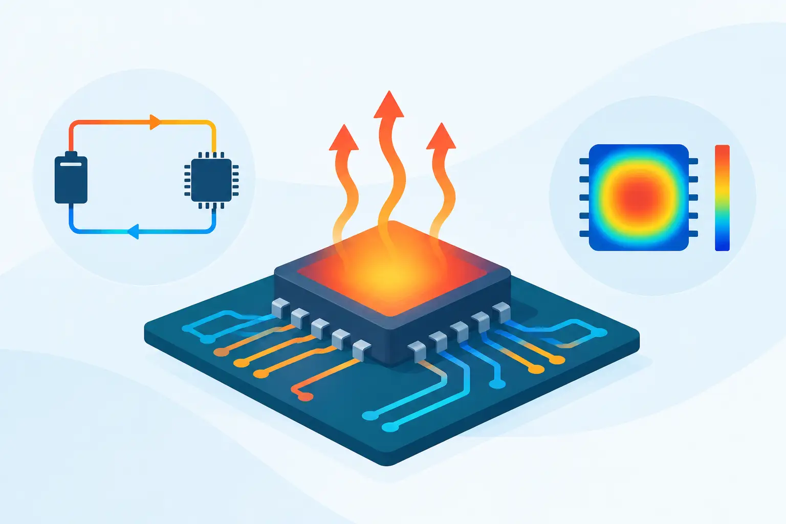
    Temperature is another frequent dividing line between a qualitative and an engineering-grade result. Temperature changes carrier concentration, mobility, intrinsic concentration, contact behavior, and thermal generation. If self-heating materially changes the local temperature, an isothermal electrical solution may not be enough. The electrical model should then be coupled to heat transfer, particularly in power structures and regions of current crowding.

    Numerical formulation is part of the model

    The equations are nonlinear and strongly coupled. Their solution requires more than assigning material properties and pressing solve. Mesh placement, discretization method, scaling, and nonlinear iteration controls determine whether the numerical answer preserves the intended physics.

    Junctions, depletion edges, thin oxides, narrow current paths, contact corners, and regions of high field deserve local mesh refinement. A coarse mesh can smear a junction and suppress the peak electric field. An unnecessarily fine mesh throughout the structure increases solve time and may make convergence more difficult without improving the quantity of interest. The appropriate mesh is tied to the output being evaluated: terminal current, peak field, local temperature, stored charge, or spreading resistance.

    For drift-dominated transport, a discretization that respects carrier flow is necessary to avoid nonphysical oscillations or negative carrier concentrations. Exponential fitting approaches, including the Scharfetter-Gummel scheme, remain widely used because they handle the transition between diffusion-dominated and drift-dominated regions effectively. Newton-based nonlinear methods can converge quickly near the solution, but bias stepping, damping, and physically reasonable initial conditions are often needed for high injection, reverse breakdown, or strongly coupled electrothermal problems.

    Mesh-convergence testing should be routine rather than reserved for publication-quality studies. Refine the critical regions and compare the engineering outputs that drive the decision. If breakdown voltage, on-resistance, or peak temperature shifts appreciably, the original discretization was not sufficient. A converged terminal current alone does not prove that an internal field solution is converged.

    Contacts and boundaries can dominate the answer

    An Ohmic contact is often modeled by fixing potential and carrier concentrations consistent with the local doping. This is reasonable only where the physical contact behaves approximately as assumed. Schottky contacts, heterojunction interfaces, surface recombination boundaries, and finite contact resistivity need boundary conditions that represent their actual carrier exchange and voltage drop.

    Contact geometry also matters. A two-dimensional cross section may accurately represent a long, uniform stripe device, but it cannot capture current spreading from a localized pad or a three-dimensional thermal escape path. In those cases, extending a two-dimensional result into three dimensions by assumption can conceal the dominant resistance or hot spot.

    This is where problem selection matters more than software breadth. A two-dimensional process and device calculation is appropriate for junction formation, cross-sectional device behavior, and many teaching or design studies. A three-dimensional solver becomes necessary when geometry controls heat flow, spreading resistance, or the electric field around localized contacts. Siborg’s MicroTec and SibLin address these workloads as separate simulation problems rather than treating dimensionality as a secondary setting.

    Where drift diffusion needs a different companion model

    The model has clear limits. At nanometer-scale channel lengths, carriers can travel over meaningful distances without reaching local equilibrium. Velocity overshoot, nonlocal transport, confinement, tunneling, and source-to-drain quantum effects can no longer be represented reliably through conventional mobility and diffusion coefficients alone. Hydrodynamic, energy-transport, Monte Carlo, or quantum-corrected approaches may be required, depending on the observable being predicted.

    High-field regions present another boundary. Drift diffusion with field-dependent mobility and impact ionization can be useful for many breakdown studies, but it may not capture hot-carrier energy distributions or nonlocal ionization accurately. The required model depends on whether the task is estimating a design margin or extracting a mechanism-sensitive reliability prediction.

    Material uncertainty can be as limiting as transport theory. Defect-rich semiconductors, novel heterostructures, irradiated devices, and poorly characterized interfaces may require calibrated trap, mobility, and boundary models before any transport formulation can produce reliable results. A more sophisticated solver cannot compensate for parameters that do not represent the material.

    Use the model to answer a defined engineering question

    The most productive workflow starts with the result that will be used: a forward I-V curve, depletion width, breakdown location, transient recovery charge, peak electric field, or temperature rise. That result determines the relevant physical models, the mesh locations that need refinement, the boundary conditions that require scrutiny, and whether two or three dimensions are justified.

    A drift-diffusion solution earns confidence when it is checked against limiting cases, mesh refinement, measured data where available, and known physical trends under bias or temperature variation. Treat it as a controlled approximation with a stated operating range. That discipline turns a fast simulation into a result that can support a device decision.

  • How to Solve Poisson Equation Numerically Well

    How to Solve Poisson Equation Numerically Well

    A Poisson solve is often the point where a physical model becomes an engineering result. Charge density becomes electrostatic potential, internal heat generation becomes temperature, and a current-spreading geometry becomes a measurable voltage field. To solve Poisson equation numerically with useful accuracy, the governing equation is only the starting point. Geometry, material interfaces, boundary conditions, mesh density, and linear-solver behavior determine whether the computed field is credible.

    For semiconductor and thermal work, the objective is not merely to obtain a converged matrix solution. It is to obtain a solution that preserves the relevant gradients, respects conservation, and remains stable when the device dimensions, material properties, or source terms change.

    The engineering form of Poisson’s equation

    The general scalar form is:

    $$nabla cdot left(k nabla uright) = -s$$

    Here, (u) is the unknown potential-like quantity, (k) is a transport or constitutive coefficient, and (s) is a volumetric source. The physical interpretation depends on the application. In electrostatics, (u) is potential and (k) is permittivity. In steady-state heat conduction, (u) is temperature and (k) is thermal conductivity. In semiconductor device simulation, the source can include ionized dopants, electrons, holes, and fixed charge.

    The constant-coefficient form, (nabla^2 u = -f), is useful for analysis and simple test cases. Real engineering models commonly require spatially varying coefficients, irregular domains, localized sources, and mixed boundary conditions. Those features are where numerical setup matters most.

    A solution is not defined by the differential equation alone. It also requires boundary conditions. A prescribed potential or temperature is a Dirichlet condition. A prescribed normal flux is a Neumann condition. A convective thermal surface or finite-contact model may lead to a Robin, or mixed, condition. Missing, inconsistent, or poorly represented boundaries are a more common source of error than the choice between two capable iterative solvers.

    How to solve Poisson equation numerically in practice

    The practical workflow begins by defining the physical domain and identifying the scale of the features that control the result. For a semiconductor cross section, these may include depletion regions, junction curvature, oxide interfaces, contact edges, or highly localized implant profiles. For thermal analysis, they may include thin layers, heat sources, vias, and boundaries between materials with very different conductivities.

    The domain is then discretized into nodes, elements, or control volumes. The continuous field equation becomes a system of algebraic equations:

    $$Amathbf{u} = mathbf{b}$$

    The matrix (A) represents the geometry, coefficients, and boundary treatment. The vector (mathbf{b}) contains source terms and contributions from specified boundaries. For a well-posed diffusion-like Poisson problem with appropriate Dirichlet conditions, this system is typically sparse and often symmetric positive definite. That structure should guide solver selection.

    Finite differences are efficient on structured rectangular or layered meshes. They are particularly appropriate when the geometry aligns naturally with Cartesian coordinates and when large regular grids are needed. Finite elements are more flexible for curved boundaries, nonuniform regions, and complex material layouts. Finite-volume formulations are attractive when local flux conservation is the principal concern.

    No single discretization is automatically superior. A structured finite-difference mesh may be faster and simpler for a planar device problem. A finite-element or finite-volume approach may better represent a curved contact, an angled interface, or a three-dimensional package feature. Pick the method that matches the problem, not a general-purpose framework that adds complexity without improving the result.

    Treat material interfaces explicitly

    At an interface, the unknown field is usually continuous, while the normal flux changes according to the coefficient on each side. For electrostatics, this means handling discontinuous permittivity correctly. For thermal analysis, it means preserving heat flux across a conductivity jump.

    A naive arithmetic average of coefficients can distort the flux when adjacent materials differ substantially. Interface-aware discretization, often using harmonic averaging in finite-volume or finite-difference schemes, is generally more appropriate for normal transport across layered materials. The correct treatment depends on the formulation and grid arrangement, but the physical requirement is clear: flux must be represented consistently across the interface.

    Refine where the field changes rapidly

    Uniform refinement is easy to implement and expensive to justify. Mesh resolution should be concentrated where gradients or sources demand it: near junctions, narrow gaps, source corners, contact edges, thin films, and material boundaries. The bulk region can often use a coarser mesh without changing the quantity of interest.

    This is not an argument for aggressive local refinement everywhere. Very abrupt changes in cell size can degrade conditioning and complicate iterative convergence. A graded mesh is usually preferable, with enough transition cells to avoid turning a local accuracy improvement into a global solver problem.

    Choose a solver based on matrix behavior

    Direct factorization methods can be effective for modest two-dimensional models and are valuable as reference solutions. Their memory use grows quickly in three dimensions because factorization introduces fill-in. A direct solve that is convenient for a small cross section can become impractical on a million-node mesh.

    For large sparse systems, iterative methods are normally the better choice. Conjugate gradient methods are suitable for symmetric positive-definite systems. GMRES or BiCGSTAB may be used when the formulation or boundary treatment produces a nonsymmetric matrix. Multigrid methods and multigrid preconditioners are especially effective for Poisson-type equations because they address error components across several length scales.

    The residual reported by a solver is necessary but insufficient. A small algebraic residual indicates that the discrete equations have been solved accurately. It does not demonstrate that the mesh is fine enough, that the source normalization is correct, or that the modeled boundaries represent the physical device. Solver tolerance should be chosen relative to the engineering quantity being extracted, such as peak electric field, contact resistance, maximum temperature, or integrated charge.

    Conditioning deserves attention. Extreme aspect ratios, large coefficient contrasts, poorly scaled variables, and pure Neumann boundaries can make the system difficult to solve. A pure Neumann problem also has an arbitrary additive constant, so a reference potential or equivalent constraint must be imposed. These are mathematical properties of the model, not software defects.

    Verify the numerical result before using it

    A credible Poisson workflow uses more than a convergence flag. Start with a case that has an analytical solution, such as a one-dimensional slab with uniform source, and verify the expected order of mesh convergence. Then test conservation by integrating fluxes and comparing them with total sources. For electrostatics, compare net boundary displacement flux with enclosed charge. For heat transfer, compare heat entering and leaving the domain with internal heat generation.

    Mesh-independence testing should focus on the reported engineering quantity. If a peak field changes by 12 percent after refinement, the original mesh was not adequate even if the average potential changed very little. Conversely, refining a region until the answer changes less than the required design tolerance is a defensible stopping criterion.

    It is also useful to inspect field plots rather than relying solely on scalar outputs. Nonphysical oscillations, discontinuities at an interface, incorrect symmetry, and unexpected extrema frequently reveal a sign error, unit mismatch, or boundary-condition mistake. In semiconductor problems, verify the sign convention for charge density and carrier terms before investigating solver settings.

    From a two-dimensional profile to a large 3D field model

    The appropriate scale depends on the decision being made. A two-dimensional model can efficiently establish diffusion profiles, depletion behavior, and lateral field effects in structures that are long in one direction. Three-dimensional analysis becomes necessary when current crowding, spreading resistance, localized heating, vias, finite contacts, or package geometry control the result.

    For these larger models, memory efficiency and sparse-solver design are not implementation details. They determine whether the simulation remains practical. SibLin v1.2 is intended for three-dimensional numerical workloads including Poisson, diffusion, heat transfer, drift-current, and spreading-resistance equations, with capacity for meshes exceeding 1,000,000 nodes. That capability matters when a simplified geometry would remove the mechanism being evaluated.

    The best numerical model is therefore not the largest available model. It is the smallest model that resolves the relevant physics, applies defensible boundaries, and demonstrates that further refinement will not change the engineering decision. Establish that discipline early, and Poisson simulation becomes a dependable part of device and thermal design rather than a source of attractive but uncertain contour plots.

  • Choosing 3D Heat Transfer Simulation Software

    Choosing 3D Heat Transfer Simulation Software

    A package temperature estimate can look acceptable while the die-level model still predicts a damaging hot spot at a contact, via array, or thin interconnect region. That difference is where 3D heat transfer simulation software earns its place. The purpose is not to generate an attractive temperature plot. It is to calculate heat flow through the actual geometry, materials, interfaces, and boundary conditions well enough to support a design decision.

    For semiconductor and electronics work, the right solver depends on the physical question. A board-level thermal estimate, a package conduction problem, and heat spreading beneath a localized device region may all be called thermal simulation, but they do not make the same demands on geometry, mesh density, equation coupling, or numerical method. Selecting a large multiphysics suite by default can add cost and workflow overhead without improving the answer. Select the simulator that matches the problem.

    What 3D Heat Transfer Simulation Software Must Solve

    At its foundation, a thermal model solves the heat equation. For steady-state conduction, this commonly takes the form of a divergence relationship between thermal conductivity, temperature gradient, and volumetric heat generation. Transient analysis adds heat capacity and time dependence. The mathematics is familiar; obtaining a useful result is not.

    Electronic structures combine dimensions that differ by orders of magnitude. A die may span millimeters, while a metal layer, insulating film, thermal boundary layer, or active region can be microns or less. Thermal conductivity can also vary substantially with material, crystal orientation, temperature, doping, and fabrication details. If the heat source is localized, the model must resolve steep temperature gradients without making the full calculation impractically large.

    A credible three-dimensional tool therefore needs more than a temperature solver. It needs a reliable way to represent spatially varying material properties, internal heat generation, complex external boundaries, and local geometric detail. It should also give the engineer sufficient control over mesh construction and convergence to determine whether an apparent hot spot is physical or numerical.

    Conduction is often the central problem

    For many chip, package, substrate, and heat-spreading studies, solid conduction dominates the question. The relevant engineering task is to find the thermal path from a heat-generating region to a defined sink, while accounting for lateral spreading, constrictions, and material transitions.

    This is particularly important when a two-dimensional cross section is no longer representative. A finite-width metal trace, discrete contact, nonuniform power distribution, asymmetric package feature, or off-center heat source introduces lateral paths that a 2D model cannot reproduce. A 3D calculation can show whether heat escapes primarily through the substrate, spreads through metallization, or accumulates near a poorly coupled interface.

    Boundary conditions determine whether the result means anything

    Thermal boundary conditions are frequently a larger source of uncertainty than the solver itself. A fixed-temperature surface can represent an idealized heat sink, but it can also conceal the thermal resistance of the path to that sink. Convective boundaries require a defensible heat-transfer coefficient and ambient reference temperature. Radiation may be relevant at exposed surfaces, but it is rarely the dominant mechanism inside a densely layered electronic assembly.

    Thermal contact resistance deserves the same scrutiny. Treating bonded layers as perfectly connected may be appropriate for one process condition and incorrect for another. If interface quality, solder coverage, adhesive thickness, or surface roughness is uncertain, evaluate a range of interface resistances rather than reporting a single precise-looking temperature.

    Match the Solver to the Physical Scope

    The most efficient simulation workflow starts by defining the question in terms of outputs, not software features. Is the needed result peak junction temperature, temperature uniformity across an active area, thermal resistance between two regions, or the sensitivity of a design change? The answer determines the appropriate domain and level of detail.

    A process or device engineer may begin with a two-dimensional profile to establish doping, diffusion, or heat-generation behavior, then require a 3D model when the lateral dimensions and spreading paths become significant. A packaging engineer may instead begin with a 3D conduction model and use a prescribed power map from electrical measurements or another device calculation. Coupled electrothermal analysis is valuable when electrical current distribution changes materially with temperature, but it should not be imposed when a fixed heat source is sufficient for the decision.

    SibLin is intended for this class of numerical work: three-dimensional heat transfer, Poisson, diffusion, drift-current, and spreading-resistance problems in a focused standalone solver. That scope matters when the engineering requirement is a large, physics-specific calculation rather than a broad enterprise environment with functions the project will not use.

    Mesh Resolution Is a Numerical Decision, Not a Display Setting

    Three-dimensional thermal models can become large quickly. Doubling the resolution in each spatial direction increases the number of cells or nodes by roughly eight times. A model that is visually detailed everywhere may consume memory and solution time without increasing confidence in the region that matters.

    The better approach is selective resolution. Refine the mesh near localized heat sources, material interfaces, narrow conduction paths, contacts, and regions where the temperature gradient is expected to be high. Use a coarser mesh in large homogeneous areas that mainly carry heat toward the external boundary. This reduces computational burden while preserving detail where the solution is sensitive.

    Mesh independence should be demonstrated, not assumed. Run the model with a baseline mesh, refine the critical regions, and compare the quantities that drive the decision: peak temperature, temperature difference between specified points, or extracted thermal resistance. If these outputs shift materially after refinement, the original mesh was not adequate. If the values stabilize, further global refinement is unlikely to be productive.

    For research and industrial studies involving 1,000,000 or more mesh nodes, solver behavior becomes especially important. The relevant question is not simply whether a program accepts a large mesh. It is whether the numerical formulation, memory use, convergence controls, and run time allow the user to complete meaningful parameter studies.

    Verify Physics Before Trusting Temperature Maps

    A converged solution is not automatically a verified solution. Numerical convergence only means the iterative process has satisfied a chosen criterion. Verification asks whether the implemented model behaves as the governing physics requires.

    Start with energy balance. For a steady-state model, the total heat leaving the domain should agree with the total internally generated heat, within a reasonable numerical tolerance. Check sign conventions at boundaries. Confirm units for thermal conductivity, power density, geometry, and heat-transfer coefficients. Errors in unit conversion can produce plausible color maps with physically impossible temperature values.

    Then compare against a limiting case. A simple slab with one-dimensional heat flow has an analytical thermal-resistance estimate. A symmetric geometry should produce a symmetric result when symmetric boundary conditions are applied. A model with zero power generation should not develop a temperature gradient without an imposed external condition. These checks are fast and often expose setup errors before significant computational time is spent.

    Measured data is the final test when it is available, but measurement comparisons also need care. A thermocouple, infrared image, electrical temperature sensor, and simulation node do not necessarily represent the same physical location or averaging volume. Compare like with like, and document the uncertainty in power dissipation, emissivity, interface properties, and ambient conditions.

    Use Parameters to Find the Design Lever

    The practical value of thermal simulation is usually not the nominal temperature result. It is the ability to identify which change reduces that temperature most effectively. Once the baseline model is checked, vary the uncertain or controllable inputs systematically.

    For a semiconductor structure, useful parameters may include heat-source location and magnitude, substrate thickness, local metallization geometry, thermal conductivity assumptions, and contact resistance. For a package-level problem, die attach thickness, interface conductivity, sink temperature, and convection conditions may dominate. Change one assumption at a time initially to understand causality, then evaluate combined cases when design interactions are expected.

    This process often reveals a result that is more useful than a single predicted junction temperature: the design may be insensitive to one expensive material upgrade but highly sensitive to a small reduction in interface resistance or a redistribution of local power. That is the type of evidence required to prioritize process changes, layout revisions, or additional measurement work.

    Questions to Ask Before Selecting a Tool

    Before licensing or deploying a thermal solver, establish whether it can represent the dimensions, governing equations, material behavior, and boundary conditions required by the intended workload. Confirm the practical mesh size on the available hardware, not only a theoretical maximum. Review how the software reports convergence and whether its output supports quantitative extraction rather than only visualization.

    Also consider the operating model. A researcher building new numerical methods may need extensive customization. An engineer evaluating a known class of heat-transfer and electrical-field problems may benefit more from a specialized application with direct setup and established algorithms. The correct choice depends on the work, the users, and the level of numerical control they need.

    A thermal model becomes valuable when it narrows uncertainty around a real engineering choice. Build the smallest model that contains the relevant physics, refine it where heat flow is most constrained, and treat every temperature result as a claim that must be checked against energy balance, mesh sensitivity, and physical evidence.