Blog

  • Thermal Simulation for Electronic Devices That Fits

    Thermal Simulation for Electronic Devices That Fits

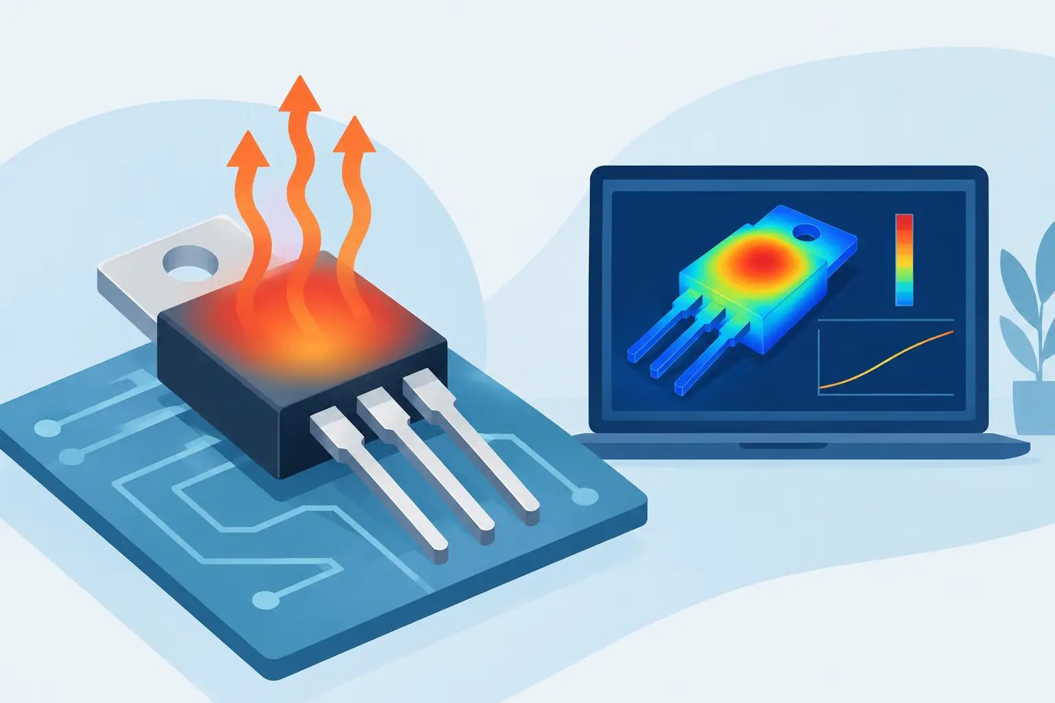
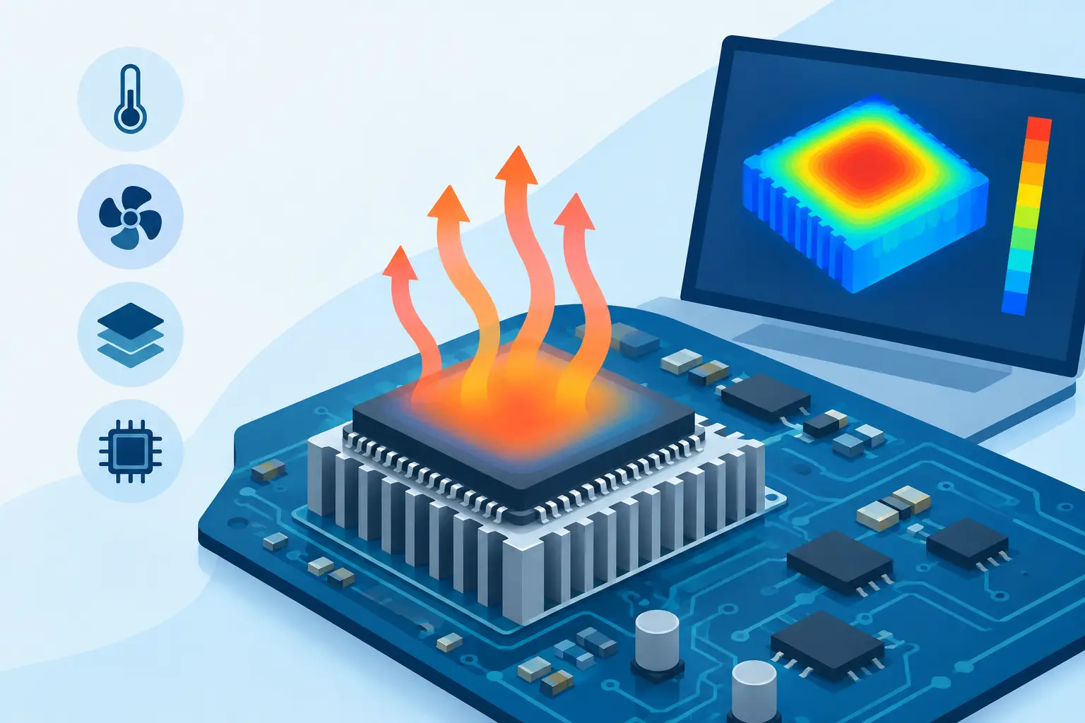
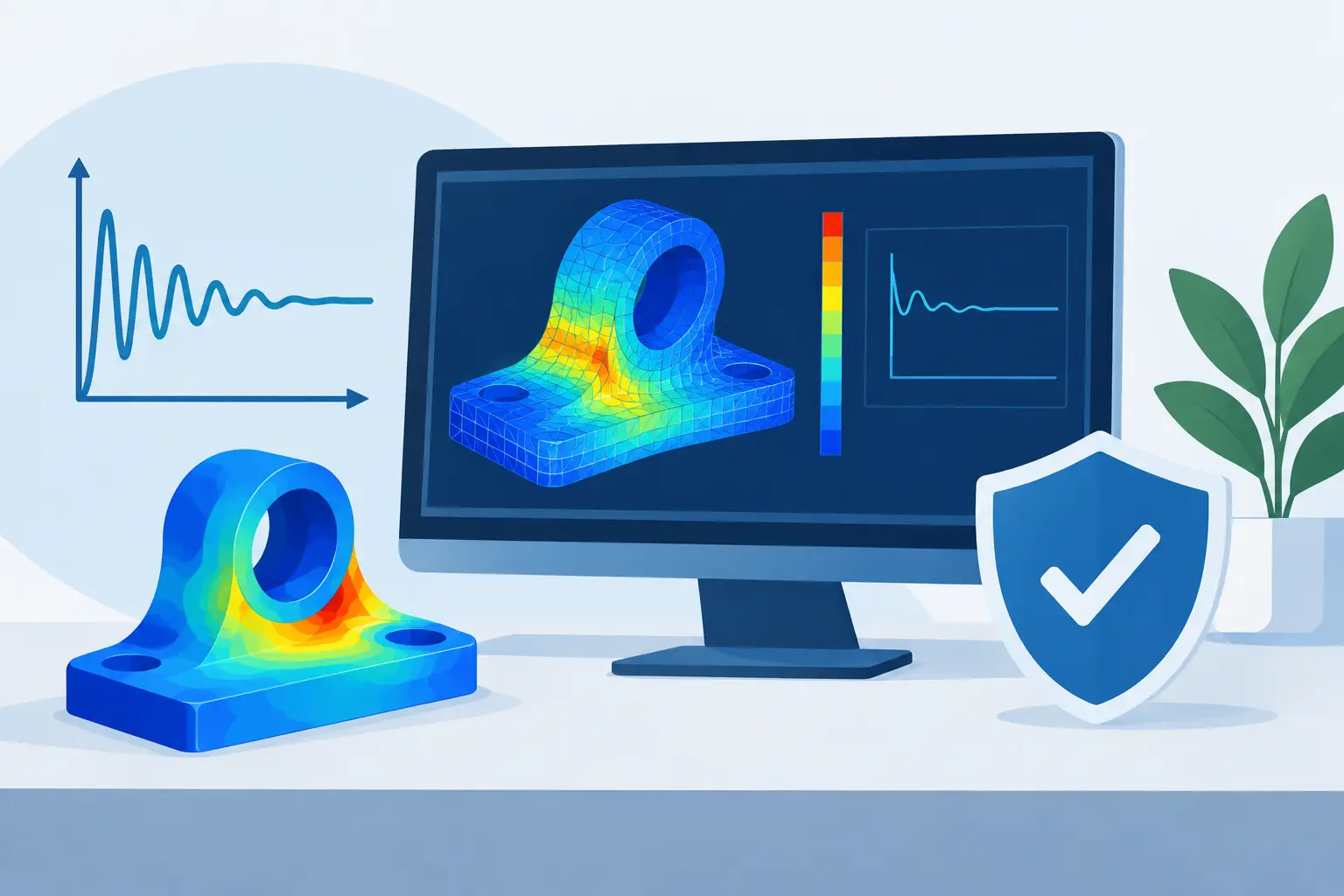
    A device can meet its electrical targets on a schematic and still fail its operating requirements after power dissipation raises the local junction temperature. That gap is where thermal simulation for electronic devices earns its place in the design workflow. The useful result is not a colorful temperature plot. It is a defensible prediction of temperature, heat flux, and thermal resistance under boundary conditions that resemble the actual package, board, and environment.

    For semiconductor and electronics engineers, thermal analysis often begins with a practical question: where is the heat generated, where can it leave, and what design change will alter the answer? The correct model depends on the scale of that question. A two-dimensional cross-section may be sufficient for a long power structure or a preliminary diffusion-related study. A three-dimensional model becomes necessary when heat spreads through finite die areas, metallization, vias, packages, heat sinks, or asymmetric boundary conditions.

    Thermal Simulation for Electronic Devices Starts With Physics

    The governing heat-transfer equation is straightforward in form, but a credible solution depends on the terms supplied to it. For steady conduction, the model balances heat generation against the divergence of heat flux. In transient work, heat capacity adds time dependence. Material thermal conductivity, density, specific heat, contact resistance, and temperature dependence can all affect the result.

    Electronic devices add complications that are easy to omit. Heat may be generated nonuniformly in an active region rather than distributed through the full silicon volume. Thin dielectric layers can impede vertical heat flow. Metal interconnects can provide lateral spreading paths. Interfaces between die attach, substrate, package, and heat sink may dominate the total thermal resistance even when their physical thickness is small.

    The electrical and thermal problems are also frequently coupled. Carrier transport produces Joule heating, while higher temperature changes mobility, resistivity, leakage, and device characteristics. In power devices, RF structures, high-current interconnects, and electrothermal sensors, treating the heat source as fixed may be an acceptable first approximation, but it is not always the final model.

    Define the Thermal Question Before the Mesh

    A large model is not automatically a better model. Before creating a mesh, define the quantity that will drive a decision. It may be maximum junction temperature, the temperature difference between two active elements, a thermal time constant, heat flux through a package interface, or spreading resistance from a small source into a substrate.

    That definition determines the geometry and the boundary conditions. A chip-level study of local self-heating may require detailed material layers near the active region but a simplified representation of the package. A module-level study may treat the die as a homogenized heat source while resolving the substrate, solder, baseplate, and cooling path. Trying to resolve every feature at every scale can consume computational effort without improving the answer to the engineering question.

    Represent heat sources where they exist

    A uniform volumetric source can be appropriate for a resistive film, a broad active area, or an early design estimate. It can be misleading for a MOSFET channel, a narrow current-crowding region, or a localized defect. If the source location is uncertain, test more than one physically plausible distribution rather than presenting a single result as definitive.

    For coupled device work, heat generation can be calculated from electrical fields and currents. For system-level studies, measured power dissipation or a specified power density may be more practical. The model should state which approach was used. This matters when comparing results across operating points or validating against measured temperatures.

    Treat boundaries as engineering inputs

    Boundary conditions can change a predicted temperature more than a moderate refinement of the mesh. A fixed-temperature boundary represents a well-controlled thermal reservoir. A prescribed heat-flux boundary represents known power transfer. Convective boundaries require a heat-transfer coefficient and ambient temperature, both of which may vary substantially with airflow, orientation, surface finish, and enclosure geometry.

    Radiation may matter for exposed high-temperature surfaces, but it is often secondary inside compact electronics assemblies. Contact resistance deserves particular attention. Assuming perfect thermal contact between assembled layers can underestimate junction temperature and conceal a packaging limitation. When interface data are uncertain, a parameter sweep is more useful than a single optimistic value.

    When 2D Is Enough and When 3D Is Required

    Two-dimensional simulation is effective when geometry, sources, and boundaries are approximately invariant along one direction. It is valuable for examining vertical heat flow through layered devices, cross-sectional current and temperature distributions, and early process or device design iterations. It also makes sensitivity studies fast enough to be used routinely rather than reserved for final verification.

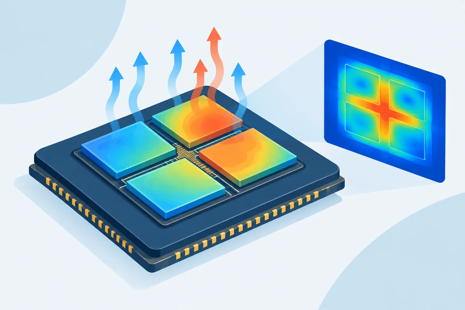
    Three-dimensional analysis is required when heat spreading is inherently spatial. Examples include finite die footprints, arrayed heat sources, bond wires, thermal vias, asymmetric metallization, edge cooling, and localized mounting conditions. A 2D result can substantially misrepresent peak temperature when it cannot capture lateral escape paths or the confinement of a small heat source.

    The choice is not always either-or. A sound workflow can begin with a 2D model to establish material sensitivities and approximate thermal resistance, then use a targeted 3D model for the regions where geometry controls the result. This approach makes model complexity proportional to the decision at stake.

    Mesh Resolution Must Follow Gradients

    Mesh density should increase where temperature gradients, material discontinuities, and source gradients are strongest. Typical refinement regions include active junctions, narrow metal traces, dielectric interfaces, via edges, and thin bonding layers. Uniformly reducing element size across a large package is rarely the most efficient route to accuracy.

    Mesh convergence should be assessed against the output of interest, not merely against the number of nodes. If maximum junction temperature changes by less than the engineering tolerance over successive refinements, further refinement may not be justified. If local heat flux or interface temperature continues to change, the model is not yet resolved for those outputs.

    For large three-dimensional problems, solver behavior matters as much as mesh construction. The numerical method must handle variable material properties, complex boundary conditions, and meshes that may exceed 1,000,000 nodes without making routine analysis impractical. Memory use, convergence criteria, and the conditioning introduced by highly contrasting conductivities are part of the modeling problem, not implementation details to ignore.

    Validate the Model in Stages

    Validation should begin with cases that have known behavior. A one-dimensional layer stack, a simple spreading-resistance geometry, or a structure with published analytical limits can reveal unit errors, boundary mistakes, and incorrect material assignments before the full model is attempted.

    Measured temperature data adds another level of confidence, but the measurement method has limits. Infrared imaging depends on emissivity and line of sight. Thermocouples disturb small structures and may measure a point away from the hottest region. Electrical temperature-sensitive parameters provide junction information but require careful calibration. Agreement is meaningful only when the experimental conditions and the simulation boundary conditions are comparable.

    A discrepancy is not automatically a solver failure. It may indicate uncertain interface resistance, incorrect heat-source placement, incomplete package geometry, or a boundary condition that does not represent the test fixture. The productive response is to identify which assumptions have enough uncertainty to explain the difference, then test them systematically.

    Select a Tool That Matches the Problem

    Thermal software should be chosen according to the equations, dimensionality, mesh scale, and workflow required. A designer studying coupled semiconductor behavior needs a different environment from an analyst calculating three-dimensional heat spreading through a package. Buying a broad software bundle does not remove that distinction.

    For users requiring a standalone three-dimensional numerical solver, Siborg Systems’ SibLin is designed for heat transfer as well as Poisson, diffusion, drift-current, and spreading-resistance problems. Its fit is strongest where engineers need direct control of a serious numerical model without adopting an enterprise suite built around unrelated workflows. For process and device studies, a separate two-dimensional tool may provide the more appropriate starting point.

    Licensing and deployment also affect practical value. A university researcher may need a model that supports instruction and repeatable graduate work. An industrial team may prioritize traceable inputs, stable solver behavior, and the ability to rerun established analyses over many design cycles. In either setting, the useful simulator is the one that produces results engineers can inspect, reproduce, and defend.

    Thermal analysis becomes most valuable when it is introduced before temperature is already a qualification failure. Build the first model around a real design decision, document the assumptions that control it, and let each refinement answer a question the previous result could not.

  • MOSFET Device Physics Simulation That Holds Up

    MOSFET Device Physics Simulation That Holds Up

    A threshold-voltage number from a compact model may be adequate for circuit exploration. It is not adequate when a process change shifts the channel profile, a high drain field changes leakage, or self-heating limits current. MOSFET device physics simulation addresses that gap by solving the physical relationships that create device behavior rather than fitting only the resulting I-V curve.

    For process engineers and device researchers, the practical value is traceability. A simulated change in threshold voltage, on-resistance, subthreshold slope, or breakdown behavior should be traceable to a doping distribution, interface condition, geometry, material property, or thermal boundary. That is the difference between a plot that resembles measurement and a model that can guide the next experiment.

    What MOSFET Device Physics Simulation Must Capture

    A useful MOSFET simulation begins with electrostatics. Poisson’s equation relates applied terminal voltages and fixed charge to the potential distribution throughout the structure. From that potential, the solver determines carrier concentrations and the formation of inversion, depletion, and accumulation regions. Gate oxide thickness, work-function difference, substrate doping, and fixed or interface charge all affect this solution.

    Carrier transport is the next requirement. In a basic operating range, drift-diffusion transport may provide the needed description of electron and hole current. The equations must account for mobility, carrier density, electric field, concentration gradients, and recombination-generation mechanisms. For many silicon MOSFET studies, this framework is the appropriate balance of physical fidelity and computational cost.

    The model must also recognize where simple assumptions stop being credible. Strong lateral fields near the drain can produce velocity saturation, mobility degradation, impact ionization, and hot-carrier effects. Short channels introduce two-dimensional electrostatics, including drain-induced barrier lowering and charge sharing. At low currents, trap-assisted generation, band-to-band tunneling, or surface leakage may matter more than the nominal channel current. The correct physics set depends on the question being asked, not on a desire to activate every available model.

    Process history is part of the device

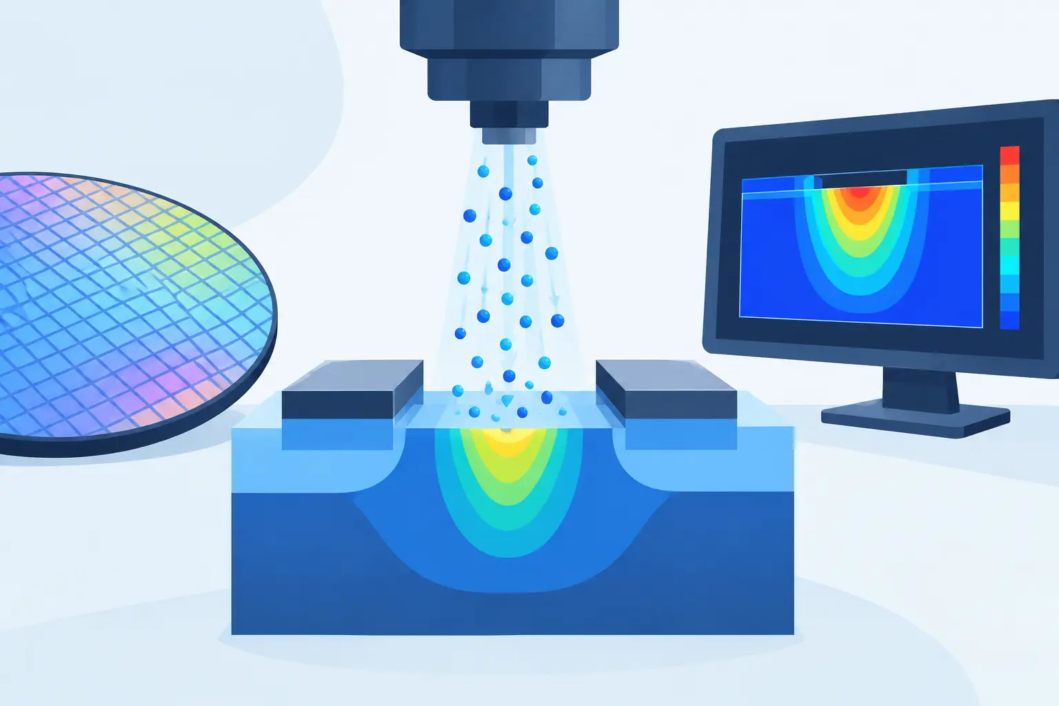
    A MOSFET is not defined by a final cross-section alone. Implant doses and energies, diffusion and activation steps, oxidation, etching, and deposited layers establish the profiles and interfaces that the device solver uses. A shallow junction with an unrealistic post-anneal profile can produce plausible-looking transfer characteristics for the wrong reason.

    This is why process and device simulation are often most effective as a connected workflow. Process simulation establishes two-dimensional dopant and material distributions. Device simulation then applies bias conditions and solves the resulting electrical behavior. When measured data disagree with the model, the engineer can test a specific physical hypothesis: a junction depth, channel dose, oxide charge, mobility parameter, or contact assumption.

    The Numerical Problem Behind a Credible Result

    MOSFET device simulation is a coupled nonlinear numerical problem. Potential changes carrier concentration; carrier concentration changes charge; charge changes potential. Current continuity equations add further coupling, particularly under high bias or when generation and recombination are active. A solver that converges quickly only when the bias step is small or the mesh is overly coarse is not necessarily providing an engineering result.

    Mesh design deserves the same discipline as model selection. Fine resolution is generally needed at the Si-SiO2 interface, junction edges, source and drain extensions, narrow current paths, and field peaks near corners. A uniformly fine mesh increases runtime and memory use without adding equivalent value everywhere. A graded mesh can resolve the regions that control the answer while keeping the overall problem manageable.

    Mesh independence should be checked for the metric that drives the decision. If the purpose is threshold-voltage extraction, refine the channel and interface until the extracted threshold stops changing materially. If the purpose is breakdown analysis, refinement must extend to the high-field region and junction curvature. One mesh is rarely optimal for every result.

    Boundary conditions require equal scrutiny. Contact placement and type, applied voltages, insulating boundaries, thermal contacts, and symmetry assumptions directly affect the solution. An ideal ohmic contact may be reasonable for one study and misleading for another. Similarly, an isothermal boundary can suppress a temperature rise that would otherwise change mobility, leakage, and power dissipation.

    Choosing Physics by Engineering Question

    The most efficient simulation plan starts with the decision that the result must support. For long-channel DC behavior, a two-dimensional drift-diffusion study with calibrated mobility and recombination models may be sufficient. It can show how channel doping, oxide thickness, or gate bias shifts threshold voltage and transconductance.

    For short-channel scaling, the study should focus on electrostatic integrity. Channel length, junction depth, spacer geometry, halo implants, and oxide thickness influence barrier control. The relevant outputs are not only drain current. They include potential contours, depletion regions, subthreshold characteristics, drain-induced barrier lowering, and the distribution of lateral electric field.

    Power and high-current devices require a broader view. Self-heating can alter carrier mobility and increase leakage, while current crowding may localize dissipation near a contact or geometric feature. Here, electrical and thermal solutions should be consistent with one another. A fixed-temperature electrical result can be useful as a first pass, but it should not be mistaken for an electrothermal prediction.

    There are cases where two dimensions are not enough. Planar MOSFET process development often fits a 2D cross-section well. Three-dimensional analysis becomes necessary when layout-dependent heat spreading, contact geometry, isolated hot spots, or nonuniform current paths dominate. The right response is not to force every problem into 3D. It is to move to 3D when the omitted dimension changes the engineering conclusion.

    Calibration Is Not Curve Fitting

    Measured data are essential, but calibration should preserve physical meaning. Start with quantities that constrain the structure: oxide thickness, sheet resistance, junction depth, dopant activation, and known dimensions. Then compare electrical observables across more than one bias condition. A model that matches one transfer curve but misses output conductance, subthreshold slope, or temperature dependence is incomplete.

    A disciplined calibration sequence usually separates process uncertainty from transport uncertainty. First establish the geometry and doping profile. Next address interface charge and work-function assumptions affecting threshold behavior. Then calibrate mobility, recombination, and high-field models against the operating regions of interest. This sequence reduces the temptation to compensate for an incorrect process profile by changing a transport parameter without physical justification.

    Sensitivity analysis adds practical value. Vary one uncertain input within a defensible range and observe the response of the selected metric. If a small uncertainty in oxide charge overwhelms the expected benefit of a channel implant adjustment, the next effort should improve the oxide or interface characterization, not refine the implant recipe. Simulation is most useful when it identifies what must be measured or controlled next.

    A Focused Toolchain Produces Better Decisions

    The simulator should match the dimensionality and equations of the problem. Engineers establishing diffusion profiles and analyzing planar device cross-sections need efficient process and device capabilities. Researchers studying heat transfer, Poisson, diffusion, drift-current, or spreading-resistance behavior in complex structures need a 3D numerical solver that can support large meshes.

    Siborg Systems approaches these workloads as distinct numerical problems rather than as features that must be purchased in a broad software bundle. MicroTec v4.23 provides two-dimensional semiconductor process and device modeling, while SibLin v1.2 addresses three-dimensional heat-transfer and field problems, including meshes exceeding 1,000,000 nodes. That separation is practical: pick the simulator that matches the problem, not a bundle you do not need.

    Tool selection should also account for the people running the study. A device physicist may need access to model details and convergence controls. A process engineer may need repeatable workflows that turn an implant and anneal sequence into profiles suitable for device analysis. Graduate researchers need transparent numerical assumptions they can defend in a thesis or publication. In each case, the result must be inspectable, not merely generated.

    What to Review Before Trusting a Result

    Before using a simulated MOSFET result in a design or process decision, review four areas: the physical structure, the selected models, numerical convergence, and agreement with independent measurements. A current-voltage plot alone does not verify any of them.

    Inspect contours of potential, carrier concentration, current density, temperature, and electric field where applicable. These plots often expose errors that terminal curves conceal, such as an unintended leakage path, a depleted contact region, or a field spike caused by mesh or geometry treatment. Confirm that further mesh refinement and smaller bias increments do not materially change the reported metric.

    Finally, state the limits of the model plainly. A simulation calibrated at room temperature and moderate drain bias should not be used without qualification to predict avalanche behavior at elevated temperature. Credible engineering work includes the operating range, assumptions, and uncertainty alongside the nominal answer.

    The useful outcome from MOSFET simulation is not a more elaborate plot. It is a defensible next action: adjust a process step, change a geometry, add a measurement, or escalate to a three-dimensional electrothermal study when the physics requires it.

  • PN Junction Device Simulation for Real Devices

    PN Junction Device Simulation for Real Devices

    A measured diode curve is the end of a chain of physical decisions: implant dose and energy, diffusion cycle, activation, contact placement, surface condition, and operating temperature. PN junction device simulation is useful when it preserves that chain rather than replacing it with an idealized depletion-region calculation. The objective is not merely to obtain a current-voltage curve. It is to determine which physical and geometrical choices produce the observed behavior, and which changes are likely to improve the device before another wafer run.

    For process engineers and device physicists, this distinction matters. An abrupt, one-dimensional junction model can establish a useful first estimate of built-in potential or depletion width. It cannot, by itself, account for lateral diffusion beneath a mask edge, nonuniform dopant activation, current crowding near a contact, or field concentration at a curved junction. Those effects often determine reverse leakage, breakdown margin, series resistance, and transient response.

    What a PN Junction Device Simulation Must Represent

    A credible simulation begins with the structure that will actually be fabricated. That normally means defining a two-dimensional cross section, substrate material and background doping, diffusion or implantation regions, oxide boundaries, metallization, contacts, and the relevant symmetry assumptions. The mesh must resolve steep dopant gradients and regions of high electric field without consuming numerical effort in uniform areas where the solution changes slowly.

    The device calculation then couples the governing semiconductor equations. Poisson’s equation establishes the electrostatic potential from ionized dopants and mobile charge. Electron and hole continuity equations describe carrier conservation. Drift and diffusion terms determine current flow under bias. Recombination-generation models provide the link between carrier populations, traps, lifetime assumptions, and leakage mechanisms.

    The required physical detail depends on the question. For a low-voltage silicon diode operated near room temperature, standard mobility and recombination models may be adequate for comparing junction depth or contact spacing. A reverse-bias leakage study may require careful treatment of depletion-region generation, surface conditions, and high-field effects. If the intended operating range includes elevated temperature, temperature-dependent intrinsic concentration, mobility, and carrier lifetime cannot be treated as secondary details.

    Model selection should be disciplined. Adding every available model does not automatically increase accuracy. It introduces parameters that may not be known independently and can obscure the reason a result changes. Use the simplest model set that represents the dominant mechanism, then add complexity when measurements or operating conditions justify it.

    The process profile is not a boundary condition

    A common source of error is treating the junction as a geometric line with assigned concentrations on either side. Real PN junctions emerge from a process history. Drive-in diffusion broadens and shifts the profile. Lateral diffusion changes the active junction geometry. Annealing affects activation and defect populations. The resulting concentration distribution is the input to the device problem, not a detail to be added later.

    This is where process and device simulation should connect directly. A process simulation can calculate a two-dimensional dopant distribution from diffusion steps, while a device solver uses that distribution to calculate equilibrium and biased electrical behavior. The engineer can then relate a shift in the thermal budget to a shift in junction depth, capacitance, leakage path, or forward voltage.

    For educational work, an analytical Gaussian or complementary-error-function profile can still be appropriate. It allows rapid examination of how concentration gradients affect junction properties. For design decisions tied to a specific mask layout and thermal sequence, process-derived profiles are usually the more defensible starting point.

    Building the Simulation Around the Engineering Question

    The most efficient PN junction device simulation starts with a stated decision. “Will this diode meet the forward-drop requirement at the specified current?” requires a different model emphasis from “Why did reverse leakage increase after a process change?” The output quantities, bias sequence, geometry, and calibration data should follow from that decision.

    For forward conduction, examine current density as well as terminal current. Terminal behavior can look acceptable while current crowds at a contact edge or narrow active region. Current-density plots reveal whether a geometry change reduces local resistance or merely moves the bottleneck. Series resistance should include the neutral semiconductor regions and contact configuration, not only the junction itself.

    For reverse bias, inspect electric-field contours, depletion expansion, generation rate, and current paths. A high-field region at a junction curvature may signal premature breakdown risk even when a one-dimensional estimate suggests adequate margin. Guard structures, lateral spacing, and contact placement can alter that result substantially.

    Capacitance analysis requires equal care. Junction capacitance varies with bias because the depletion region changes width. In practical structures, lateral components and parasitic overlap capacitance may contribute significantly. A simulation that reports only an ideal planar junction capacitance can be useful for screening, but it should not be presented as the total device capacitance without considering layout.

    Use calibration as an engineering loop

    Simulation is strongest when it is compared against data at more than one operating point. A single fitted forward-voltage point can hide incorrect assumptions about mobility, contact resistance, active area, or lifetime. Compare measured and calculated current-voltage behavior across the relevant range, then examine capacitance-voltage data, sheet resistance, spreading resistance, or junction-depth measurements where available.

    Calibration should proceed from quantities with fewer ambiguities to those with more coupled causes. Process information and measured doping profiles constrain the starting structure. Resistance data helps constrain electrically active regions and contacts. Forward and reverse curves then test transport and generation assumptions. If a model matches only after physically implausible parameter changes, the geometry or process profile may be wrong.

    This approach also clarifies uncertainty. Semiconductor simulation does not eliminate process variation. It identifies which uncertain inputs have meaningful leverage on the result. A sensitivity study of junction depth, background concentration, lifetime, and contact resistance can show whether the design is limited by an inherent physical trade-off or by a parameter that needs better measurement.

    Numerical Choices Affect Physical Credibility

    The equations governing a biased PN junction are nonlinear and strongly coupled. Near equilibrium, the numerical task is relatively gentle. Under large forward bias, reverse bias, or near breakdown, carrier concentrations and fields can vary by many orders of magnitude across a small region. An inadequately resolved mesh or poorly controlled nonlinear iteration can produce nonphysical oscillations, false convergence, or a smooth-looking result that is not reliable.

    Mesh refinement should follow gradients, not visual preference. Refine near the metallurgical junction, surface interfaces, contact edges, and anticipated high-field locations. Then verify that further refinement does not materially change the quantities used for the design decision. Terminal current alone is not enough for this check. Peak field, local generation rate, and current-density distribution may remain mesh-sensitive after the I-V curve appears stable.

    Bias stepping is equally practical. Solving equilibrium first and advancing voltage in manageable increments usually provides a better initial condition for each subsequent solution. Difficult operating regions may require smaller steps. This is not a workaround for weak physics. It is a controlled method for following a nonlinear solution branch.

    A focused standalone tool is often preferable when the workload is specifically two-dimensional process-to-device analysis. MicroTec, for example, is designed to model semiconductor processes and devices without requiring users to assemble an oversized software suite. For three-dimensional thermal, electrostatic, diffusion, drift-current, or spreading-resistance problems, the relevant solver should be selected on its mesh capacity and equation set rather than its product category.

    Knowing When Two Dimensions Are Enough

    Two-dimensional analysis is often the right first tool for a long diode stripe, a repeated cross section, or a structure whose dominant variation lies in one plane. It allows rapid examination of process profiles, junction curvature, and contact spacing with a computational cost that supports parameter studies.

    Three-dimensional simulation becomes necessary when current spreads in two lateral directions, contact geometry is localized, thermal paths are genuinely three-dimensional, or the device layout contains corners and isolated features that cannot be represented by a cross section. The decision is not ideological. If a 2D model captures the dominant gradient and produces stable, calibrated trends, it is usually the efficient choice. If it suppresses the mechanism under investigation, a 3D calculation is required.

    The practical value of PN junction device simulation lies in shortening the distance between a physical hypothesis and a testable design change. Build from a process profile, solve the appropriate transport problem, verify numerical stability, and compare against measurements. The resulting model becomes more than a diode curve: it becomes a controlled way to decide which fabrication or layout change deserves the next experiment.

  • Choosing a Two Dimensional TCAD Simulator

    Choosing a Two Dimensional TCAD Simulator

    A two dimensional TCAD simulator is most useful when the question is not simply whether a device will operate, but why its electrical behavior follows from its fabrication history and geometry. Junction depth, lateral diffusion, oxide growth, dopant activation, depletion width, and terminal bias all interact. A credible simulation must carry those dependencies from process steps into device equations without forcing the engineer to build a larger model than the problem requires.

    For many semiconductor development tasks, two dimensions are the appropriate level of abstraction. A 2D cross-section can capture the governing physics of planar transistors, diodes, resistors, isolation structures, and process test vehicles while keeping mesh size, setup time, and interpretation under control. The practical objective is not to buy the largest software suite. It is to select the simulator that matches the engineering question.

    What a two dimensional TCAD simulator should solve

    A useful 2D TCAD workflow connects process simulation to device simulation. On the process side, the software should model the operations that establish a device structure: substrate definition, deposition, etching, oxidation, implantation, diffusion, and annealing. These steps create the material boundaries and dopant distributions that determine later electrical performance.

    On the device side, the simulator must solve the coupled electrostatic and carrier-transport problem. Poisson’s equation establishes the potential distribution from charge, while electron and hole continuity equations describe carrier motion under diffusion and drift. Depending on the device and operating regime, physical models for recombination, mobility, incomplete ionization, and high-field effects may also matter.

    The connection between these stages is where practical value is created. A nominal junction depth or sheet resistance entered by hand may be adequate for an early estimate. It is not equivalent to carrying a calculated two-dimensional dopant profile through to a current-voltage, capacitance-voltage, or breakdown analysis. Process history often explains effects that a simplified device-only structure misses, particularly near mask edges, contact regions, shallow junctions, and isolation boundaries.

    Geometry is not merely a drawing

    In a 2D model, geometry defines more than the visible device outline. It sets material interfaces, electrode placement, boundary conditions, and the regions where gradients become severe. An oxide edge, a curved depletion region, or a narrow current path can require local mesh refinement even when the rest of the structure is comparatively uniform.

    The right simulator should let the user represent these features directly and inspect the resulting structure before relying on electrical results. A visually plausible cross-section is not sufficient. Engineers should be able to verify layer thicknesses, material regions, net doping, and mesh distribution, because an error in any of these inputs can appear later as an apparently physical result.

    Match the simulator to the decision being made

    The first selection question is whether the problem is fundamentally two-dimensional. If the structure is uniform in one direction, or if the key mechanism is evident in a cross-section, 2D simulation generally provides the necessary fidelity at a manageable computational cost. This is common in process development, teaching laboratories, device design studies, and parameter investigations.

    A fully three-dimensional model becomes justified when out-of-plane geometry changes the answer. Examples include nonuniform contacts, localized heating, current crowding around complex layouts, vias, package paths, and structures whose width is comparable to their critical lateral dimensions. In those cases, reducing the problem to a cross-section can conceal the dominant mechanism rather than simplify it.

    That distinction should guide procurement as well as analysis. A research group studying a process sequence and its influence on a planar device should not be required to adopt a broad multiphysics bundle if a focused 2D process and device tool addresses the work. Conversely, a team solving large three-dimensional thermal or field problems should use a solver designed for that workload. Dimensionality is an engineering choice, not a feature checklist item.

    Start with observables, not model count

    Before comparing products, define the result that will support a decision. It may be a threshold-voltage trend after a change in implant energy, a reverse-bias leakage mechanism, a capacitance curve, a lateral diffusion profile, or the sensitivity of breakdown behavior to junction curvature.

    Then work backward. Identify the process steps that establish the relevant structure, the transport equations required, the bias conditions to be applied, and the quantities to be extracted. This approach prevents two common errors: selecting a tool because it advertises many models that the project will not use, or using an oversimplified model because the desired output was never stated precisely.

    More physical models do not automatically produce a more useful answer. Each model introduces parameters, assumptions, and calibration needs. For a comparative study under controlled conditions, a disciplined baseline model may reveal a trend more clearly than a heavily parameterized setup. For correlation to measured production data, additional physics and careful calibration may be necessary. The appropriate level depends on the device, the available measurements, and the consequence of being wrong.

    Numerical methods determine whether results can be trusted

    TCAD is not only a collection of semiconductor equations. It is a numerical solution of coupled, nonlinear equations over a discretized structure. This matters when depletion regions are narrow, doping changes abruptly, bias sweeps approach breakdown, or carrier concentrations span many orders of magnitude.

    Mesh quality is central. A coarse mesh can suppress the gradients that control electric field, current density, and charge distribution. An excessively fine mesh everywhere increases solution time without improving the regions that matter. The productive approach is targeted refinement at junctions, interfaces, electrode edges, and other locations with steep spatial variation.

    Convergence behavior deserves equal attention. A solution that converges quickly to the wrong branch is not a good solution, and a model that fails near the operating point of interest is not useful simply because it worked at zero bias. Engineers should be able to control bias stepping, inspect intermediate solutions, and recognize when a result reflects numerical limitations rather than device physics.

    Validation should proceed in stages. Verify the process structure first: dimensions, profiles, and material boundaries. Next, check equilibrium quantities such as potential and carrier distributions. Finally, compare terminal characteristics and extracted values with analytic expectations, published references, or measured data where available. This staged method isolates errors far more efficiently than attempting to diagnose an unexpected I-V curve after the full workflow is complete.

    A practical workflow for process and device studies

    The strongest workflows are reproducible. A study should preserve its process sequence, geometry definitions, material parameters, meshing choices, physical models, bias conditions, and extraction method. That record lets another engineer reproduce the result and lets the original author determine which change caused a shift in performance.

    For process engineers, begin with a small set of measurable profile targets. Simulate the diffusion or implantation sequence, inspect the resulting two-dimensional concentration distribution, and adjust assumptions only when there is a physical or measured basis. Once the structure is credible, transfer it into device analysis rather than recreating an approximate profile manually.

    For device engineers, use controlled parameter sweeps. Change one process variable, geometric dimension, or material parameter at a time when establishing sensitivity. Combined sweeps are useful later, but they can obscure causality at the start. Record not only the final extracted metric but also field plots, current paths, and carrier distributions. These internal quantities often explain a trend before it becomes visible in terminal data.

    For teaching and research, the same discipline applies. A 2D model is particularly effective for showing how fabrication choices translate into electrostatics and transport. Students can compare idealized and process-derived structures, observe the effect of mesh placement, and learn why a simulated result requires physical interpretation rather than blind acceptance.

    Where a focused standalone tool fits

    A focused simulator is often preferable for teams that need repeatable semiconductor process and device analysis without dedicating staff to maintaining a large enterprise environment. The essential requirements are clear physical coverage, stable numerical algorithms, usable structure and mesh control, and outputs that support engineering interpretation.

    Siborg’s MicroTec v4.23 is positioned for this type of two-dimensional process and device modeling. It supports engineers working from initial diffusion-profile studies through electrical device analysis, while retaining the direct workflow expected in an instructional or industrial R&D setting. The relevant evaluation standard remains the same: confirm that the tool represents the structures, equations, and outputs required by the project before expanding scope.

    Licensing and deployment should also match the actual user group. An individual engineer, a small device team, and a university laboratory have different needs, but all benefit from a tool that can be installed, understood, and used consistently over the life of a project. Long-term utility comes from repeatable analyses and credible results, not from unused modules.

    Use 2D simulation to reduce uncertainty

    The best use of a two-dimensional TCAD simulator is to reduce uncertainty before fabrication, measurement, or redesign. It can show whether a proposed process change is likely to move a junction, alter an electric-field peak, or change a terminal characteristic enough to justify further work. It can also identify which dimensions or process variables deserve tighter experimental control.

    Treat the model as an engineering instrument. Build it from known structure and physics, test it against independent evidence, and increase complexity only when the decision requires it. When the model and the question are matched carefully, two dimensions can provide a clear and defensible basis for the next design or process step.

  • How to Simulate Dopant Diffusion in TCAD

    How to Simulate Dopant Diffusion in TCAD

    A diffusion simulation can look credible while being wrong in the quantity that matters most: junction depth, sheet resistance, peak concentration, or lateral encroachment beneath a gate edge. To understand how to simulate dopant diffusion, treat it as a calibrated process-modeling problem rather than a contour-plot exercise. The required inputs are the implant or deposited dopant profile, the thermal history, the material state, and a numerical mesh capable of resolving the gradients produced by each step.

    Start with the physical question

    The simulation setup should follow the engineering decision it must support. For a CMOS well drive, the concern may be final vertical junction depth and concentration under the active region. For a source/drain process, lateral diffusion and overlap with the gate can dominate device behavior. For a discrete power device, the relevant target may be a deep, lightly doped drift region with a specified resistivity profile.

    These cases do not require the same domain size, mesh density, or diffusion model. Defining acceptance quantities before constructing the model prevents a common failure mode: spending time refining plots that do not answer a process or device question.

    At minimum, identify the dopant species, substrate orientation and background concentration, initial profile source, anneal sequence, ambient, and temperature ramp. Also decide which outputs will be compared with measurements or process targets. Typical choices are the concentration profile at selected locations, metallurgical junction depth, sheet resistance, active dose, and lateral diffusion distance.

    Build a defensible initial dopant profile

    Dopant diffusion begins with the concentration distribution present before the thermal cycle. That distribution may come from ion implantation, constant-source predeposition, limited-source deposition, epitaxial growth, or an imported measured profile. Its accuracy sets the ceiling for the later diffusion result.

    For implanted boron, phosphorus, arsenic, or antimony, an analytic or tabulated as-implanted profile should represent projected range, straggle, dose, tilt effects where relevant, and any masking geometry. A simple Gaussian approximation can be useful for early design studies, but it may not represent channeling tails or the near-surface behavior of a real implant. If the implant profile has been characterized experimentally, use that information instead of compensating for a poor starting profile with arbitrary diffusivity adjustments.

    For furnace diffusion, distinguish between predeposition and drive-in. During a constant-source predeposition, the surface concentration can approach the solid solubility limit for the process temperature. During a limited-source drive-in, the total dose is conserved while the profile broadens and the peak concentration falls. Confusing these boundary conditions changes both the profile shape and the junction depth.

    In two-dimensional process simulation, geometry belongs in the initial setup as well. Oxide thickness, openings in masks, silicon topography, and neighboring regions influence where dopants enter and how they diffuse laterally. A one-dimensional calculation remains valuable for profile calibration, but it cannot predict edge effects.

    Select the diffusion physics to match the regime

    The simplest diffusion model is based on Fick’s law:

    [ frac{partial C}{partial t} = nabla cdot left(Dnabla Cright) ]

    where (C) is dopant concentration and (D) is diffusivity. With a constant diffusivity, this model offers useful intuition and can be adequate for lightly doped, limited cases. Semiconductor process conditions frequently require more.

    Diffusivity is strongly temperature dependent and is commonly represented by an Arrhenius relationship, (D = D_0exp(-E_a/kT)). A small temperature error at high anneal temperature can therefore produce a meaningful junction-depth error. Use the actual thermal schedule, including ramp-up, soak, and cool-down periods when their thermal budget is significant.

    At higher concentrations, diffusion can become concentration dependent. Point defects, Fermi-level effects, dopant clustering, and transient enhanced diffusion after implantation can alter the effective rate and the electrically active dopant concentration. Boron diffusion after an implant anneal is a familiar example where interstitial-mediated transient effects can matter. Arsenic and phosphorus can require attention to clustering and activation at high concentrations.

    The correct level of physics depends on the process window and the required accuracy. A compact model may be appropriate for establishing a preliminary process profile. If the result will be used to set implant energy, anneal time, or a critical device dimension, use a calibrated model that includes the mechanisms demonstrated to affect that process. More physics is not automatically better if model parameters are unavailable or cannot be validated.

    Use a mesh that resolves junctions and interfaces

    Numerical diffusion solvers compute concentration on a mesh, so mesh placement has direct physical consequences. Refine the mesh where concentration changes rapidly: near the silicon surface, at implant peaks, around pn junctions, beneath mask edges, and at material interfaces. The mesh can be coarser in regions where the concentration is nearly uniform and far from the area of interest.

    An excessively coarse mesh smears the profile numerically, making a junction appear deeper or a peak lower than the process predicts. Excessive refinement everywhere increases solve time without adding useful accuracy. The practical test is mesh convergence: reduce local element size, rerun the case, and confirm that the reported junction depth, sheet resistance, and peak concentration change by less than the tolerance needed for the decision.

    Mesh quality matters especially in two dimensions. Narrow windows, curved corners, and thin oxide layers can create poorly shaped elements or abrupt size transitions. These can reduce solver efficiency and obscure whether an observed feature is physical or numerical. Refine locally and transition gradually into the surrounding domain.

    Run the thermal sequence as process steps

    A diffusion model should represent the actual sequence, not a single equivalent anneal unless equivalence has been established. Oxidation may inject point defects and consume silicon. An intervening etch can alter boundary conditions. A rapid thermal anneal and a long furnace drive-in can deliver similar nominal thermal budgets while producing different activation and diffusion behavior.

    Set each step with its duration, temperature, ambient, and applicable surface or interface conditions. Track dose conservation where a closed-system drive-in is expected. For constant-source diffusion, verify that the imposed surface condition is physically plausible at the selected temperature. In implanted processes, evaluate activation separately from total chemical concentration when the device simulation requires electrically active dopants.

    A useful workflow is to first calibrate a one-dimensional vertical profile against a known process monitor, then transfer the validated thermal and diffusion parameters to the two-dimensional geometry. This separates core diffusion calibration from lateral effects and reduces the number of uncertain variables adjusted at once.

    Validate against measurements, not only expectations

    A simulation is calibrated when it reproduces independent observables within an agreed tolerance. Secondary ion mass spectrometry can provide concentration-versus-depth data, although interpretation near the surface and at low concentrations requires care. Spreading-resistance profiling, sheet-resistance measurements, electrochemical capacitance-voltage profiling, and junction-stain measurements can provide complementary constraints.

    Do not calibrate only to junction depth. Different profiles can cross the background concentration at the same depth while having different peak concentration, dose, and electrical activation. A stronger comparison uses several quantities: profile shape, sheet resistance, junction position, and, where possible, lateral encroachment. If one parameter set fits a predeposition monitor but not a drive-in monitor, the issue may be the selected physics or boundary condition rather than a single diffusivity value.

    Document the parameter set, source data, mesh settings, and thermal schedule used for each calibrated case. That record is what turns an individual run into a reusable process model for design teams, researchers, and future process revisions.

    Choose the simulator for the dimensionality of the problem

    A one-dimensional solver is efficient for rapid studies of vertical profiles and thermal-budget sensitivity. Once mask edges, isolation structures, or source/drain geometry affect the result, a two-dimensional TCAD process simulator is the appropriate tool. It should support process sequencing, dopant diffusion models, mesh control, and direct inspection of concentration contours and extracted profiles.

    MicroTec is designed for two-dimensional semiconductor process and device modeling, making it suitable for establishing and examining diffusion profiles without requiring a broad software bundle. The useful criterion is not the size of the software suite. It is whether the simulator represents the physical mechanisms and geometry needed for the process decision.

    Before relying on a final profile, run one controlled sensitivity study. Vary temperature, anneal time, mesh density, and the uncertain diffusion parameter within credible bounds. If the predicted junction remains stable, the simulation can support a firm decision. If it moves substantially, the next productive step is usually better process data or measurement calibration, not a more elaborate plot.

  • What Is Semiconductor Processing in Chip Fabrication?

    What Is Semiconductor Processing in Chip Fabrication?

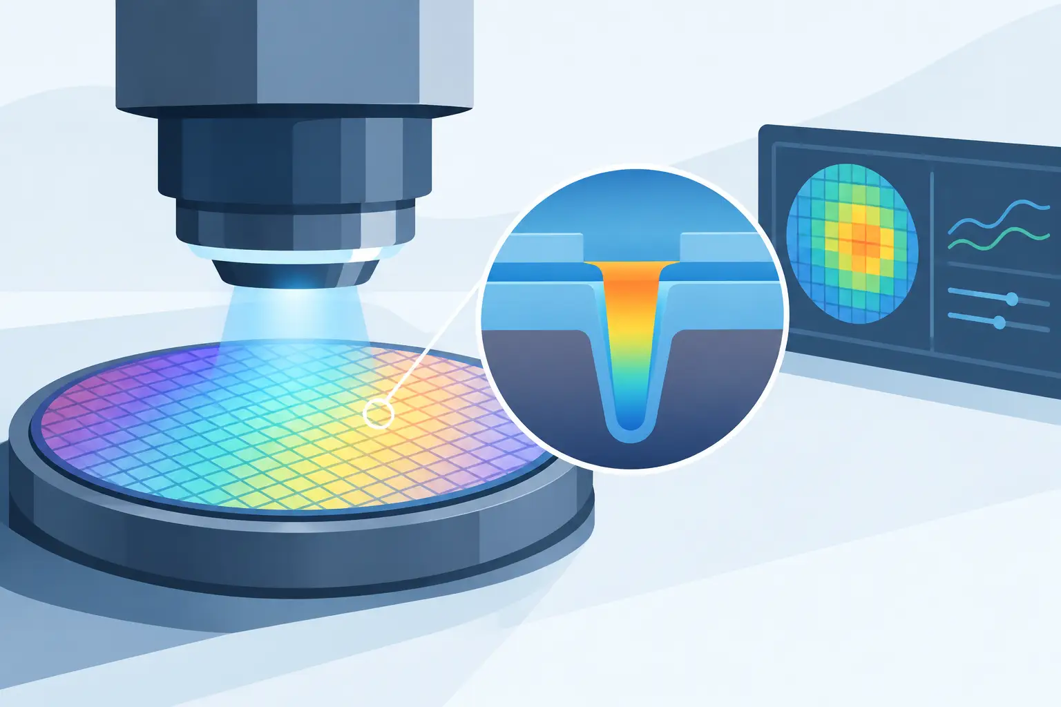
    A transistor layout is only an intention until semiconductor processing turns it into controlled material structure on a silicon wafer. For engineers asking what is semiconductor processing, the useful answer is not simply “chip manufacturing.” It is the ordered set of physical and chemical operations used to create active devices and interconnects with dimensions, dopant concentrations, film properties, and alignment tolerances that must remain within specification across an entire wafer.

    The process links device physics to manufacturing reality. A device designer may specify a threshold voltage, junction depth, contact resistance, or gate dielectric thickness. Process integration must determine which thermal cycles, deposition methods, lithographic masks, etches, implants, and cleaning steps can produce those results repeatedly.

    What Is Semiconductor Processing?

    Semiconductor processing is the fabrication of electronic devices by selectively modifying semiconductor wafers. Silicon is the most common starting material, although silicon carbide, gallium nitride, gallium arsenide, indium phosphide, and other materials are used where their electrical, optical, thermal, or high-voltage characteristics justify the added process complexity.

    A typical wafer moves through hundreds or thousands of individual operations. These are not independent steps. Each one changes the conditions for the next. An oxidation may consume silicon and alter dimensions. An ion implant establishes a dopant distribution, but a later anneal changes its depth and electrical activation. An etch creates the intended feature geometry, yet can also introduce sidewall damage or leave residues that affect a subsequent deposition.

    The result is a layered structure containing transistors, diodes, resistors, capacitors, isolation regions, contacts, and metal interconnects. In integrated-circuit production, these structures are repeated many times across a wafer and later separated into individual dies. In discrete power devices, sensors, and optoelectronic components, the sequence and geometry differ, but the same principle applies: controlled material modification creates useful electronic behavior.

    The Core Operations in Semiconductor Processing

    The exact flow depends on the device, material system, feature size, and fabrication facility. Still, most process flows are built from a common set of operations.

    Wafer preparation and thermal processing

    Manufacturing begins with a polished wafer that must meet demanding requirements for crystal quality, flatness, particle contamination, and surface condition. Initial cleaning removes organic residues, metals, particles, and native oxides that could create defects or cause poor film adhesion.

    Thermal processing then changes the wafer through high-temperature exposure. Thermal oxidation, for example, grows silicon dioxide that can serve as an insulating layer, a masking layer, or part of a gate structure. Diffusion drives dopant atoms into the wafer through elevated-temperature exposure. Annealing repairs crystal damage after implantation and electrically activates dopants.

    Temperature history is central to process control. Dopant movement is cumulative, so every high-temperature step can alter a previously established profile. A process engineer is therefore concerned not only with peak temperature but also with ramp rates, dwell time, ambient chemistry, and the full thermal budget.

    Thin-film deposition

    Devices require films that are conductive, insulating, semiconducting, or protective. Common deposition approaches include physical vapor deposition, chemical vapor deposition, atomic layer deposition, electroplating, and epitaxial growth.

    Film selection is governed by more than nominal thickness. Engineers assess uniformity across the wafer, step coverage over topography, density, stress, stoichiometry, impurities, electrical resistivity, dielectric constant, and interface quality. A film that is acceptable on a flat monitor wafer may fail in an actual device if it does not cover narrow trenches or high-aspect-ratio features adequately.

    Epitaxy is a special case in which a crystalline layer is grown with a defined relationship to the substrate. It is particularly important for structures requiring controlled doping and low defect density, including some power devices, bipolar devices, and compound-semiconductor components.

    Photolithography and pattern transfer

    Photolithography defines where subsequent processing will occur. The wafer is coated with photoresist, exposed through a mask or reticle, and developed to leave a patterned resist image. That pattern becomes a temporary stencil for etching, implantation, deposition, or lift-off.

    Critical lithographic concerns include linewidth, overlay accuracy, focus, exposure dose, resist profile, and defect density. Overlay error is especially consequential in multilayer devices because features on one layer must align correctly with features already present below it. As dimensions shrink, small variations in pattern placement can change transistor length, parasitic capacitance, or contact overlap.

    Lithography does not create the final device structure by itself. It transfers geometric information into a process mask. The following etch, implant, or deposition determines how that information becomes physical material geometry.

    Etching and material removal

    Etching selectively removes material from exposed regions. Wet etches use liquid chemistries and may be isotropic or crystallographically selective. Dry etches use plasma-based processes and can provide the anisotropy needed for vertical sidewalls and fine patterns.

    Selectivity, etch rate, profile control, uniformity, and endpoint detection all matter. An etch must remove the target film without damaging the underlying layer or excessively consuming the mask. Plasma conditions may also affect electrical performance through charging damage, residue formation, or altered surface chemistry.

    The trade-off is often direct. A highly anisotropic process can preserve critical dimensions but may have lower selectivity or introduce more sidewall effects. A gentler wet process may provide excellent selectivity but lack the directional control required for advanced interconnect or transistor features.

    Doping and junction formation

    Doping establishes n-type and p-type regions by adding controlled concentrations of donor or acceptor atoms. Ion implantation is widely used because it provides dose control and can be spatially patterned using photoresist or hard masks. Diffusion remains useful in certain processes and is fundamental to understanding how dopant profiles evolve during thermal treatment.

    The key output is not merely dopant dose. Device behavior depends on the final electrically active concentration as a function of depth and lateral position. Implant energy, dose, tilt, channeling, pre-amorphization, anneal conditions, and nearby material boundaries can all affect the result.

    For a MOS device, changes in channel doping and junction profiles can shift threshold voltage, leakage, breakdown behavior, and series resistance. For a power device, vertical doping profiles often determine the trade-off between on-resistance and blocking voltage. These are problems where process simulation is valuable because electrical performance cannot be inferred from mask geometry alone.

    Metallization, planarization, and passivation

    Once device regions are formed, contacts and interconnects connect them into circuits. This stage can involve barrier layers, metal deposition, patterning, dielectric deposition, via formation, and copper electroplating. Modern multilevel interconnect requires careful control of resistance, capacitance, electromigration risk, and contact integrity.

    Chemical-mechanical planarization removes topography so later lithographic levels remain within focus requirements. It is a necessary capability for complex multilayer structures, but it introduces its own sources of variation, including dishing, erosion, and within-wafer nonuniformity.

    A final passivation layer protects the device from moisture, contamination, and mechanical damage. Pad openings are then created for wire bonding, flip-chip attachment, probing, or other packaging methods.

    Why Process Integration Is a Physics Problem

    Process integration is the discipline of making individual modules work as a coherent device flow. A successful deposition recipe is not enough if its film stress causes pattern distortion. A correct implant may still produce the wrong junction after downstream oxidation and annealing. A low-resistance contact can become unreliable if the cleaning sequence leaves interfacial contamination.

    This is why semiconductor processing relies on coupled physical models. Diffusion and oxidation affect geometry and concentration profiles. Poisson and drift-current equations connect those profiles to electrical behavior. Heat transfer becomes important in anneals, high-power devices, packages, and reliability studies. Mechanical stress and thermal expansion can also influence film integrity and device characteristics.

    Simulation is most useful when it answers a bounded engineering question: whether a proposed thermal cycle produces the required two-dimensional dopant profile, how a process change affects a junction, or whether a three-dimensional structure can dissipate heat within a specified temperature limit. Siborg Systems develops standalone tools for these distinct workloads, including two-dimensional process and device simulation and three-dimensional numerical analysis of heat transfer, Poisson, diffusion, and drift-current problems.

    From Process Flow to Measured Device Performance

    No process model replaces measurement. Fabrication teams use test structures, monitor wafers, metrology, electrical characterization, defect inspection, and reliability testing to determine whether the physical wafer matches its intended design. Thickness measurements, sheet resistance, critical-dimension data, implant monitoring, capacitance-voltage curves, and current-voltage measurements each expose different parts of the process.

    The practical objective is correlation. A model should be checked against measured profiles and device data, then used to reduce the number of experimental iterations required for the next design or process revision. The appropriate model detail depends on the decision being made. Early development may require fast estimates of diffusion behavior; failure analysis may justify a detailed two-dimensional or three-dimensional solution.

    Semiconductor processing is therefore best understood as controlled cause and effect. Every material change has a physical consequence, and every electrical specification imposes constraints on the process sequence. Engineers who preserve that connection between fabrication conditions, material structure, and measured device behavior make better use of both wafer experiments and simulation.

  • Semiconductor Process Modeling That Supports Decisions

    Semiconductor Process Modeling That Supports Decisions

    A diffusion profile is not merely an intermediate process result. It determines junction depth, sheet resistance, electric-field distribution, and ultimately whether a device meets its electrical targets. Semiconductor process modeling gives engineers a controlled way to examine those dependencies before committing material, masks, furnace time, or fabrication runs.

    The value is not in producing a visually convincing cross section. It is in establishing a numerical representation of the fabrication sequence that is accurate enough to guide a decision: adjust the implant condition, change a drive-in schedule, revise an oxide thickness, or determine whether a proposed process window can produce the required device behavior.

    What semiconductor process modeling must represent

    A useful process model begins with the physical sequence used to form a device. Depending on the technology, that sequence may include substrate preparation, oxidation, dopant introduction, diffusion, annealing, etching, deposition, and metallization. Each step changes the material structure or impurity distribution that later device calculations must use.

    For many silicon devices, dopant transport is central. An initially implanted or deposited concentration profile evolves under thermal treatment through diffusion. The result is affected by temperature, time, diffusivity, boundary conditions, concentration dependence, and interactions with the surrounding structure. A model that assumes a simple one-dimensional profile can be sufficient for an early estimate, but it becomes inadequate when lateral diffusion, mask edges, overlapping wells, or localized geometry affect the device.

    Process simulation also needs to account for geometry. A shallow junction below a wide opening behaves differently from a similar junction near a narrow feature, where lateral transport changes the final profile. Oxide growth consumes silicon and moves interfaces. Etching and deposition alter boundaries that affect later thermal and electrical calculations. The process flow must therefore be represented as a connected physical history, not as a collection of isolated parameter values.

    From process conditions to device behavior

    The practical purpose of semiconductor process modeling is to provide inputs for device analysis. Once the simulator has established the structure, material regions, and impurity distributions, those results can be used to calculate electrical behavior through equations such as Poisson, carrier continuity, and drift-current relations.

    This connection matters because electrical specifications are often expressed in terms that fabrication steps do not directly control. A process engineer may set implant dose and energy, diffusion temperature, or oxidation time. A device engineer may need threshold voltage, breakdown margin, current capability, capacitance, or leakage behavior. Modeling creates a common technical basis between those views.

    Consider a junction intended to reduce series resistance without pushing the depletion region into an unwanted area. Increasing the thermal budget may lower peak concentration and drive dopants deeper. That may improve one resistance-related metric while worsening punch-through behavior or changing capacitance. There is no universally correct direction for the change. The appropriate choice depends on the device architecture, voltage range, target geometry, and acceptable process variation.

    A two-dimensional process and device model is particularly valuable when lateral effects are part of the question. It can show whether the final junction contour beneath a mask edge is compatible with the intended current path, isolation region, or gate structure. For planar technologies and instructional device structures, two dimensions often provide the required physics with substantially less computational overhead than a full three-dimensional model.

    Model fidelity should follow the engineering question

    The most detailed model is not automatically the most useful model. Semiconductor process modeling must balance physical fidelity, available calibration data, runtime, and the decision at hand.

    At the earliest design stage, an engineer may only need to establish approximate two-dimensional diffusion profiles and assess whether a proposed sequence is physically plausible. In that case, a compact model with well-defined inputs can be more productive than a large simulation environment requiring extensive setup. The aim is to reject unsuitable conditions quickly and identify the parameters that deserve closer study.

    As development progresses, the requirements change. Measured sheet resistance, junction depth, or concentration data can be used to calibrate the model. The calibrated process result can then support device calculations across a range of bias conditions and dimensions. Calibration is not an optional finishing step. It determines whether the simulation is a predictive engineering tool or simply a qualitative illustration.

    Three-dimensional analysis becomes justified when the physics is inherently three-dimensional. Examples include heat flow through complex layouts, spreading resistance near contacts, nonuniform current distribution, or structures where the out-of-plane dimension cannot be represented by a reasonable approximation. In those cases, simplifying the geometry may hide the mechanism under investigation. The cost is a larger mesh, greater memory demand, and a more careful numerical setup.

    The practical rule is direct: choose the simulator that matches the problem, not a bundle of capabilities that will not be used. A two-dimensional process model should not be forced to answer a three-dimensional thermal question. Conversely, a million-node three-dimensional calculation is unnecessary when a calibrated two-dimensional process and device analysis can resolve the design choice.

    Numerical methods determine whether results can be trusted

    Process modeling is governed by coupled nonlinear physical relationships and by numerical choices that affect stability and accuracy. Mesh resolution, time stepping, boundary conditions, discretization method, convergence criteria, and material parameters all influence the solution.

    Mesh placement deserves particular attention. Fine resolution is needed near shallow junctions, oxide-silicon interfaces, sharp concentration gradients, and narrow geometric features. Applying that resolution uniformly across a large domain can make calculations unnecessarily expensive. A well-constructed mesh places computational effort where the gradients require it while retaining an efficient representation elsewhere.

    Boundary conditions can be equally consequential. A fixed concentration at a surface, a zero-flux boundary, and an interface condition each imply different physical assumptions. If those assumptions are not consistent with the actual process, an apparently stable simulation can still produce misleading profiles. Engineers should document the conditions used, especially when comparing simulations with process measurements or transferring models between projects.

    Parameter uncertainty should be treated explicitly. Furnace temperature variation, implant uncertainty, material-property assumptions, and geometry tolerances can each affect the final result. Rather than relying on a single nominal run, evaluate a bounded set of conditions around the intended process. This identifies whether a design has useful margin or depends on a narrow operating point that fabrication may not maintain.

    A disciplined workflow for process simulation

    A reliable workflow begins by defining the decision the model is intended to support. “Simulate the process” is not sufficiently specific. A better objective is to determine the thermal cycle needed to reach a target junction depth, assess the effect of lateral diffusion on isolation, or generate a structure for threshold-voltage analysis.

    Next, define the smallest geometry and physics set that can answer that question. Establish material regions, process steps, dopant species, thermal conditions, and relevant boundaries. Use known measurements where available, and keep assumptions visible rather than embedding them in undocumented defaults.

    Run baseline cases first. Inspect the resulting geometry and concentration contours before proceeding to electrical analysis. A device calculation based on an incorrect junction location or material boundary may converge numerically while describing the wrong structure. Intermediate inspection is faster than diagnosing an unexpected electrical result after several additional simulation stages.

    Then vary the parameters that the process can actually control. For a diffusion study, those may include thermal time and temperature. For an implanted structure, dose, energy, and anneal conditions may be more relevant. Compare outputs in engineering terms: junction depth, peak and surface concentration, sheet resistance, lateral encroachment, or the device metric derived from the final profile.

    Finally, compare the model with measurements at the level appropriate to the project. Exact agreement at every point is rarely attainable, particularly when input material data are incomplete. The objective is a model that reproduces the behaviors needed for design decisions and clearly identifies where uncertainty remains.

    Selecting tools for the workload

    For engineers who need two-dimensional fabrication and device analysis, MicroTec v4.23 is designed for semiconductor process and device modeling without requiring users to become full-time TCAD specialists. It supports the progression from process definition and diffusion profiles to device-level physical analysis, making it appropriate for development work and semiconductor education.

    When the problem moves beyond planar process behavior into three-dimensional heat transfer, electrostatics, diffusion, drift-current, or spreading resistance, a dedicated numerical solver is the more appropriate choice. SibLin v1.2 addresses these classes of problems on meshes exceeding 1,000,000 nodes, where dimensionality and mesh scale are part of the engineering requirement rather than optional detail.

    The distinction is useful for procurement as well as analysis. Separate tools can allow an organization to license the calculation capability it needs, keep workflows focused, and avoid imposing an oversized environment on researchers whose work is limited to a defined physical problem.

    A process model earns its place in a development flow when it narrows uncertainty before fabrication. Start with the physical question, calibrate against the measurements that matter, and use the dimensionality required by the mechanism under study. That approach produces results engineers can act on, not just simulations they can display.

  • Choosing Semiconductor Process and Device Simulation Software

    Choosing Semiconductor Process and Device Simulation Software

    A process simulator earns its place long before the first wafer is run. Semiconductor process simulation software lets an engineer test whether a proposed implant, diffusion, oxidation, deposition, or etch sequence can produce the intended structure and electrical behavior before committing material, tool time, and mask revisions.

    That value is straightforward, but selecting the right simulator is not. A package optimized for a full foundry-scale flow can be excessive for an engineer establishing a two-dimensional dopant profile. Conversely, a simplified educational tool may not provide the physical models, numerical control, or output required for device development. The correct choice begins with the physical problem, not with the largest available software bundle.

    Start With the Engineering Question

    Process simulation is often described as a single activity, yet the underlying questions differ substantially. One project may require the evolution of a boron profile during successive thermal steps. Another may need to determine how oxidation changes a device geometry, then carry that structure into electrical device analysis. A third may be validating whether a process modification shifts junction depth, sheet resistance, threshold voltage, or breakdown behavior outside an acceptable range.

    These questions define the required model scope. If the objective is a preliminary diffusion profile, a focused two-dimensional process calculation may be sufficient. If process changes must be connected to terminal characteristics, the simulator must support a credible path from process structure to device solution. If the issue is thermal spreading in a package or a large three-dimensional conductive region, process TCAD alone is not the appropriate tool. The governing equations, dimensionality, and mesh scale have changed.

    This distinction matters because simulation results are only useful when their assumptions are visible. A fast calculation based on the wrong transport model or boundary condition can create more confidence than insight. Engineers should be able to identify which physical mechanisms are represented, which are approximated, and whether those choices are appropriate for the decision at hand.

    What Semiconductor Process Simulation Software Must Model

    At a minimum, useful process simulation software represents geometry evolution and impurity redistribution with enough fidelity to support the intended design decision. The necessary detail depends on the technology and process step. Ion implantation may require models for projected range, dose, damage effects, and subsequent annealing. Diffusion requires treatment of concentration-dependent diffusivity and, where relevant, interactions with point defects or oxidation. Oxidation, epitaxy, deposition, and etching introduce additional geometry and material considerations.

    The question is not whether every model available in the literature is included. It is whether the implemented model set is technically defensible for the process window being studied. For mature silicon technologies, a validated and well-understood model set can be more productive than an expansive environment that demands extensive calibration before a useful run can be completed.

    From Process Structure to Device Behavior

    A process model is often an intermediate result rather than the final answer. The practical output is a structure containing material regions, junction locations, impurity distributions, and geometrical features that affect electrical operation. Device simulation then uses that structure to solve the relevant semiconductor equations, typically including Poisson and carrier continuity relations with drift and diffusion current components.

    This process-to-device connection is especially useful when a process change has indirect electrical consequences. A deeper junction may reduce one risk while increasing parasitic capacitance. A thermal cycle may improve activation while changing lateral diffusion near a critical edge. Simulation cannot remove such trade-offs, but it makes them available for examination before fabrication.

    For many development tasks, two-dimensional modeling remains the practical starting point. Cross-sectional structures capture the dominant physics in a wide range of planar devices, diffusion studies, and instructional applications while keeping mesh generation and computation manageable. Three-dimensional analysis becomes necessary when the physical layout itself controls the result, such as complex current spreading, localized heating, or nonuniform thermal paths.

    Numerical Method Is a Product Requirement

    A simulator’s graphical interface and model list are visible during evaluation. Numerical behavior becomes visible later, often when the project reaches its most difficult case. Convergence stability, mesh quality, boundary-condition handling, and solution control determine whether a result can be reproduced and trusted.

    Semiconductor equations are strongly coupled and can become numerically demanding around sharp doping gradients, material interfaces, depletion regions, and high-field conditions. A credible tool must provide algorithms suited to these conditions, not merely produce a contour plot for an easy example. The user should be able to refine the mesh where gradients require it, examine intermediate structures, and determine whether a result has changed materially with numerical resolution.

    Mesh size is not a badge of capability by itself. An unnecessarily dense mesh can increase solution time without improving the engineering conclusion. An overly coarse mesh can conceal critical features. The useful question is whether the software permits a mesh strategy that is proportional to the geometry and physics. For large three-dimensional thermal, electrostatic, diffusion, or spreading-resistance problems, capacity also matters. A solver designed for meshes exceeding 1,000,000 nodes addresses a different class of workload than a compact process simulator.

    Evaluate the Workflow, Not Just the Physics List

    A technically complete tool that requires specialized support for routine changes can become a bottleneck. Most engineering teams need to alter a dose, thermal budget, layer thickness, or device dimension; rerun the model; compare profiles or electrical characteristics; and document the basis for the decision. The workflow should support that cycle without imposing unnecessary infrastructure.

    Standalone licensing can be a meaningful advantage for groups with targeted analysis needs. It allows a process engineer, device researcher, or university laboratory to use the simulator that matches the work instead of acquiring a broad suite with capabilities that will remain unused. This is not always the right procurement model. Organizations operating a large, integrated design environment may value enterprise integration, centralized administration, and standardized data flows. For focused process and device studies, however, direct access to a specialized simulator can reduce both cost and operational friction.

    Training requirements should be evaluated honestly. A tool should not require every user to become a full-time TCAD specialist before they can obtain a reliable first result. At the same time, no simulator eliminates the need for engineering judgment. Users still need to define the physical assumptions, verify input parameters, inspect meshes, and compare predictions against measurement. Good software makes these responsibilities manageable rather than hiding them.

    Verification Is More Than a Benchmark Plot

    Before using simulation for a design or manufacturing decision, establish a verification routine. Start with cases that have measured junction depths, sheet resistances, capacitance-voltage data, current-voltage curves, or thermal measurements. Compare the prediction with the quantity that actually matters to the project, not only with a visually similar profile.

    Disagreement does not automatically mean the software is unsuitable. It may reveal uncertainty in a process parameter, an incomplete thermal history, a measurement limitation, or a model assumption that does not hold for the technology. The useful response is to isolate the discrepancy. Sensitivity studies can show whether the outcome is dominated by dose, time, temperature, geometry, contact conditions, or another parameter.

    For university and research use, this process also has educational value. Students can see how physical assumptions and numerical resolution affect an answer rather than treating simulation as a black box. For industrial teams, the same discipline produces models that can be reused and defended across design reviews.

    Match Dimensionality to the Dominant Physics

    Two-dimensional process and device simulation is appropriate when the structure can reasonably be represented by a cross section and the main gradients lie in that plane. It is efficient for studying diffusion profiles, implants, wells, junctions, and many conventional device geometries. A focused tool such as Siborg’s MicroTec is intended for this category of process and device modeling, where practical setup and reliable numerical results matter as much as model coverage.

    Three-dimensional simulation should be selected when reducing the geometry to two dimensions would alter the conclusion. Heat flow through an asymmetric structure, electrostatic fields around a localized feature, current spreading, and complex diffusion paths are common examples. Here, a three-dimensional solver must address the relevant equation set, which may include heat transfer, Poisson, diffusion, drift-current, and spreading-resistance equations.

    The transition from 2D to 3D is not automatically an upgrade. It introduces greater meshing effort, memory demand, and solution time. Use 3D because the engineering problem requires it, not because it appears more complete.

    A Practical Selection Standard

    The most effective selection process is deliberately narrow. Define the device or process question, identify the governing physics, determine whether 2D or 3D representation is necessary, and set acceptance criteria based on measurable outputs. Then test a representative problem with realistic geometry and parameters. A demonstration based only on idealized examples will not reveal the limitations that matter in production research.

    Ask whether the tool produces results that can be checked, whether its numerical controls are accessible, and whether the licensing model fits the people who will actually use it. Review technical documentation and evidence of long-term use in industrial and academic settings. Established adoption does not replace validation for a specific process, but it is a relevant indicator that the software has supported real engineering workloads.

    The right simulator is the one that makes the next technical decision clearer: whether a diffusion profile is acceptable, whether a process change alters device behavior, or whether a three-dimensional thermal path needs redesign. Choose the tool that answers that question with appropriate physics and numerical discipline, then keep the model tied to measurement as the work advances.

  • Welcome to the Semiconductor Process and Device Simulation Blog

    a dedicated space for process engineers, device physicists, researchers, and academic educators exploring the frontiers of semiconductor modeling.

    As device architectures scale and thermal power densities increase, technology computer-aided design (TCAD) and 3D field solvers have become critical for reducing costly physical tape-outs. This blog focuses on practical, physics-driven simulation methods that bridge the gap between high mathematical accuracy and everyday engineering usability.

    What We Cover

    • Industrial R&D: Streamlining process optimization, modeling 2D dopant diffusion profiles, analyzing 3D thermal transport, and mitigating drift-current spreading resistance in power and microelectronic devices.
    • Academic & Educational Application: Bringing core device physics to life in university classrooms (from UC Berkeley to Waseda University) with intuitive simulation tools that let students focus on physics rather than complex software setup.
    • Efficient Tooling: Insights on leveraging lightweight, robust standalone solvers like MicroTec (2D process/device simulation) and SibLin (3D thermal and field solving) capable of running 1,000,000+ mesh node calculations without heavy server infrastructure.

    Whether you are designing next-generation power electronics or teaching fundamental device physics, subscribe or follow along for technical deep-dives, simulation tutorials, and industry insights.